Dielectric composition for thin-film transistors

Active Publication Date: 2015-07-07
XEROX CORP
View PDF17 Cites 2 Cited by
  • Summary
  • Abstract
  • Description
  • Claims
  • Application Information

AI Technical Summary

Benefits of technology

[0009]Disclosed in embodiments are electronic devices and processes for making such electronic devices. Generally, the dielectric layer is formed from a dielectric composition as described herein that contains an infrared (IR) absorber or IR absorbing agent. During the curing process, this composition allows the dielectric composition to attain higher temperatures than the other components of the electro

Problems solved by technology

These curing temperatures and times are, in most ca

Method used


Image

  • Dielectric composition for thin-film transistors
  • Dielectric composition for thin-film transistors
  • Dielectric composition for thin-film transistors

Examples


examples

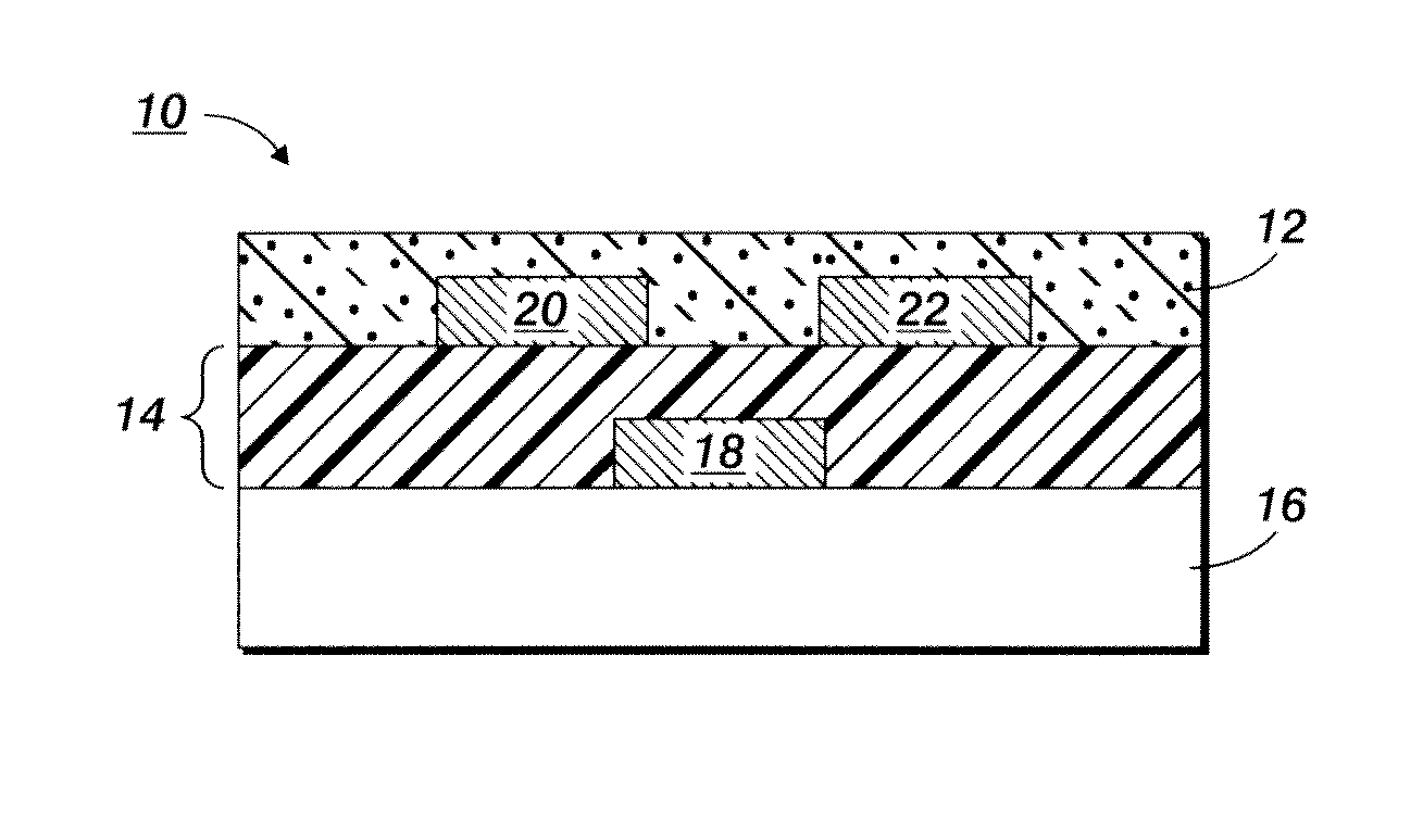
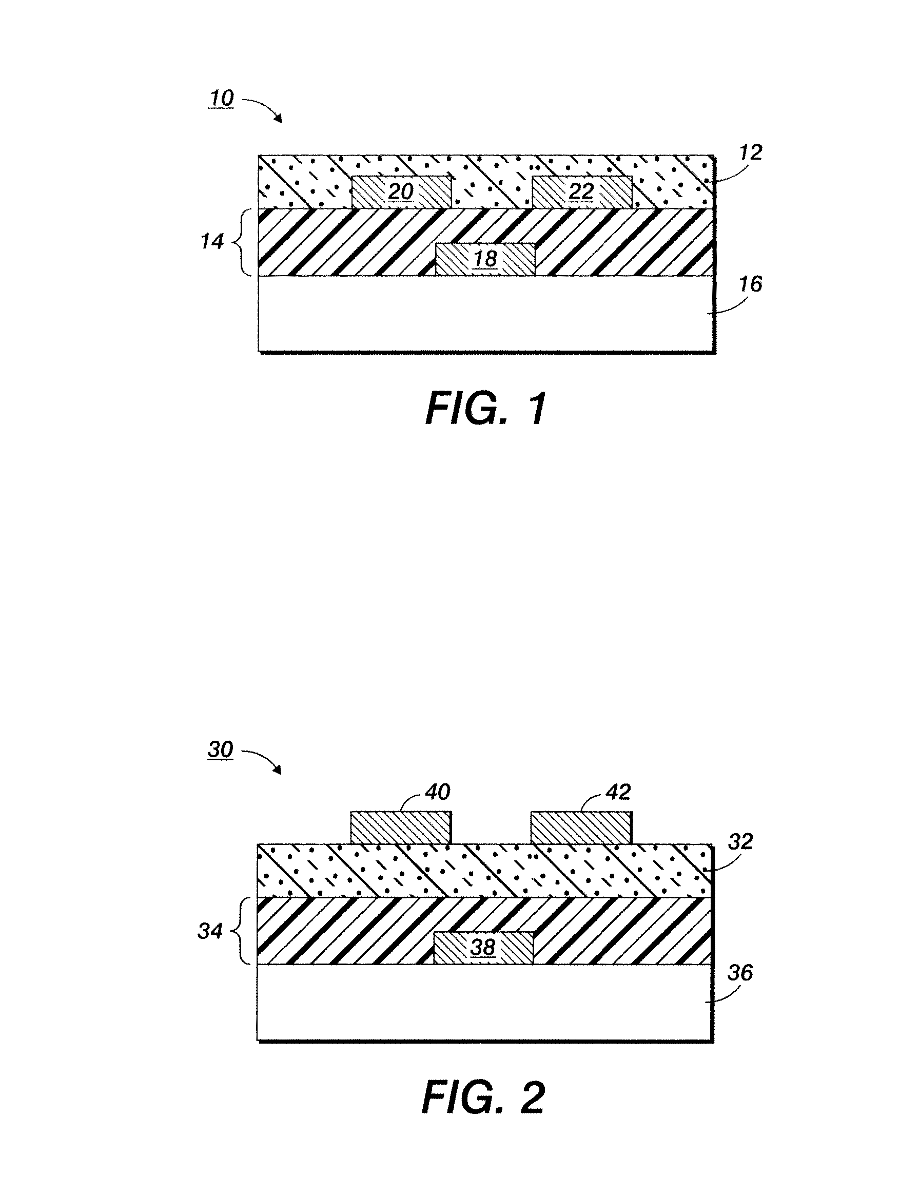
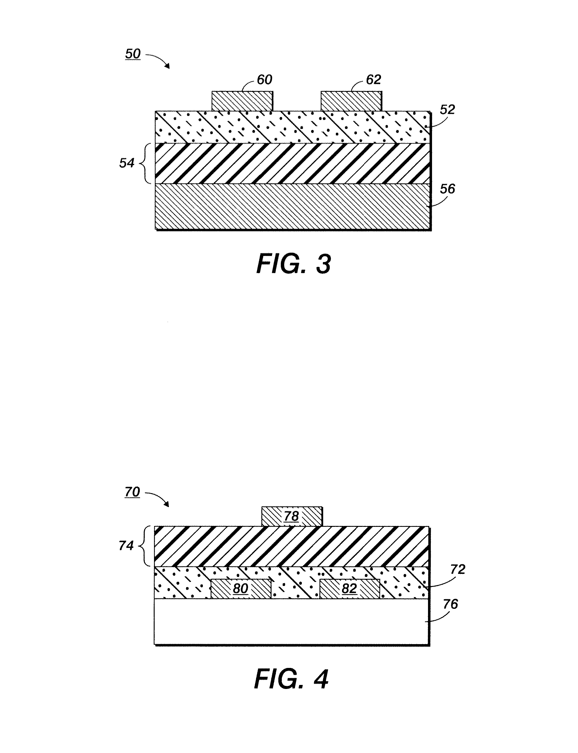
[0090]A substrate made of PET and having a thickness of 3 mils (0.003 inches, 76.2 microns) was provided. A thin layer of aluminum functioned as the gate electrode.

[0091]A dielectric composition was prepared that contained poly(methyl silsesquioxane), poly(4-vinyl phenol), a crosslinking agent, an infrared absorbing agent, and a solvent. 0.08 grams poly(4-vinyl phenol) (Aldrich, Mw=25000) was dissolved in 1.0 grams n-butanol. 0.08 grams methylated melamine-formaldehyde resin (Aldrich, 84 wt % in n-butanol) and 0.12 g poly(methyl silsesquioxane) (26 wt % in n-butanol) were added to the mixture. 0.003 grams infrared absorbing agent (ADS815EI, American Dye Source, Inc.) was also added. After filtering through a 0.2 μm syringe filter, the dielectric composition was spin coated onto the substrate at 2000 rpm for 60 seconds. The deposited dielectric composition was put on top of a hotplate at 80° C. and irradiated with an infrared lamp on top for 5 minutes to form a dielectric layer. It w...


PUM

PropertyMeasurementUnit
Nanoscale particle sizeaaaaaaaaaa
Temperatureaaaaaaaaaa

Abstract

An electronic device, such as a thin-film transistor, includes a substrate and a dielectric layer formed from a dielectric composition. The dielectric composition includes a dielectric material, a crosslinking agent, and an infrared absorbing agent. In particular embodiments, the dielectric material comprises a lower-k dielectric material and a higher-k dielectric polymer. When deposited, the lower-k dielectric material and the higher-k dielectric material form separate phases. The infrared absorbing agent allows the dielectric composition to attain a temperature that is significantly greater than the temperature attained by the substrate during curing. This difference in temperature allows the dielectric layer to be cured at relatively high temperatures and/or shorter time periods, permitting the selection of lower-cost substrate materials that would otherwise be deformed by the curing of the dielectric layer.

Description

BACKGROUND[0001]The present disclosure relates, in various embodiments, to thin-film transistors (TFTs) and / or other electronic devices comprising a gate dielectric layer. The gate dielectric layer is formed from a dielectric composition as described herein that contains an infrared (IR) absorber or IR absorbing agent. This allows the dielectric composition to be selectively cured while its substrate remains at a relatively lower temperature, preventing deformation of the substrate.[0002]TFTs are generally composed of, on a substrate, an electrically conductive gate electrode, source and drain electrodes, an electrically insulating gate dielectric layer which separate the gate electrode from the source and drain electrodes, and a semiconducting layer which is in contact with the gate dielectric layer and bridges the source and drain electrodes. Their performance can be determined by the field effect mobility and the current on / off ratio of the overall transistor. High mobility and h...

Claims


Application Information

Patent Timeline
IPC IPC(8): H01L21/31H01L51/05H01L21/268H01L51/00C08K5/00
CPCH01L51/052H01L21/268H01L51/0003H01L51/0036H01L51/0537H01L51/0545C08K5/0041C08K5/0091H10K71/12H10K85/113H10K10/478H10K10/471H10K10/464H10K10/466
Inventor WU, YILIANGLIU, PINGWIGGLESWORTH, ANTHONY JAMESHU, NAN-XING
Owner XEROX CORP
Why Eureka
Try Eureka