
Semiconductor device

a technology of semiconductor devices and semiconductors, applied in semiconductor devices, semiconductor/solid-state device details, solid-state devices, etc., can solve the problems of high cost of conventional gold wire connection, and insufficient high temperature storage life and high temperature operating life of metals other than gold, so as to achieve less wear.

Inactive Publication Date: 2015-07-14
SUMITOMO BAKELITE CO LTD
View PDF25 Cites 1 Cited by
  • Summary
  • Abstract
  • Description
  • Claims
  • Application Information

AI Technical Summary

Benefits of technology

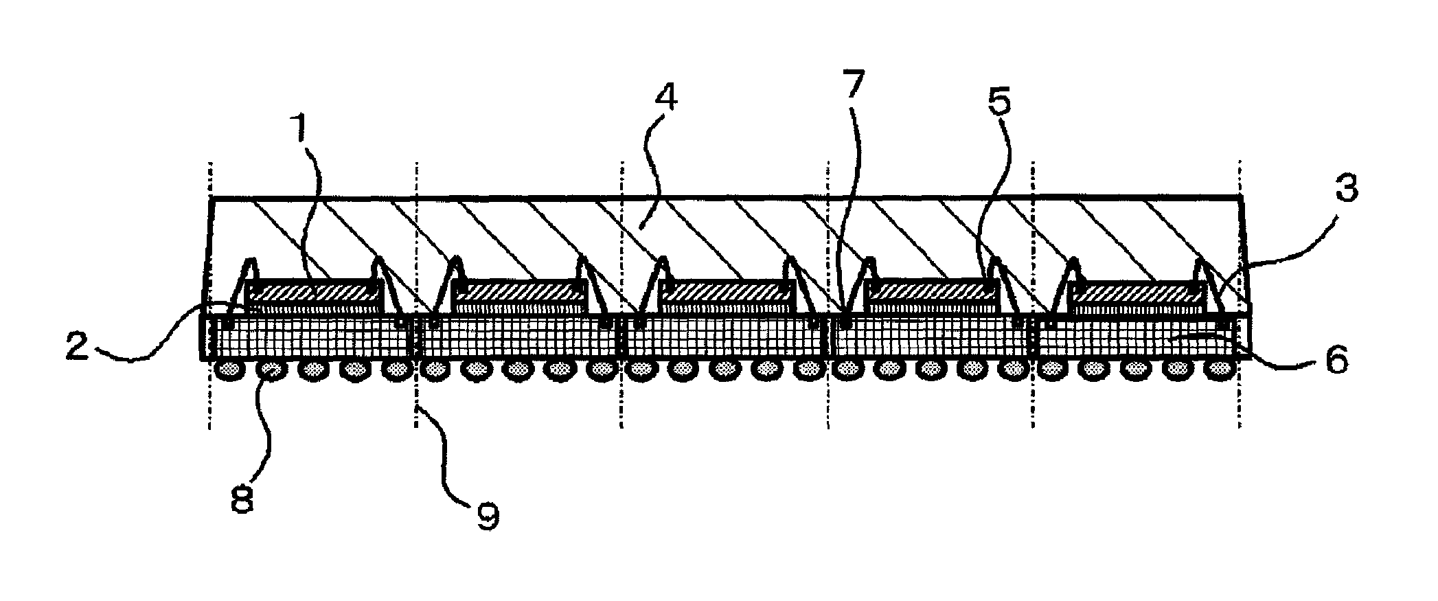
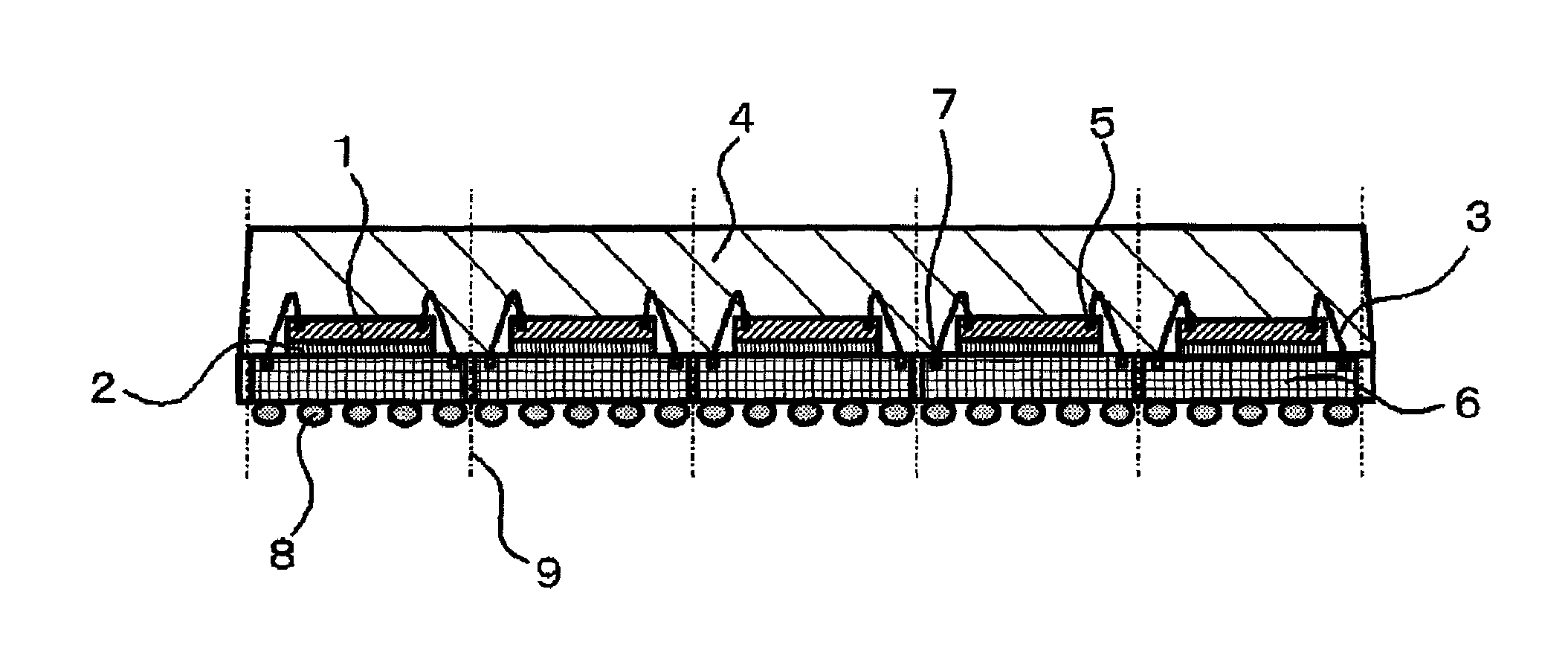
The present invention provides a semiconductor device that is easy to segment after encapsulation and molding, has less worn cutting blades, and has high reliability in high temperature storage life, operating life, and moisture resistance. The semiconductor device consists of a lead frame or circuit board, a semiconductor element, a copper wire, and an ep epoxy resin composition for the encapsulating material, which is molded at one time and then segmented into pieces. The copper wire, which connects the semiconductor element to the lead frame or circuit board, is not easily corrosed, and the semiconductor device has excellent balance among the various reliability parameters.

Problems solved by technology

On the other hand, because the demand for cost reduction on semiconductor devices is also strict and the cost of the conventional gold wire connection is high, connection with use of metals other than gold such as aluminum, a copper alloy and copper is also employed.
However, metals other than gold are still insufficient in the high temperature storage life and high temperature operating life under the high temperature environment having a temperature exceeding 150 degrees centigrade, which are especially demanded in the automotive applications, and the electrical reliability such as the moisture resistance reliability under the high temperature and high humidity environment having a temperature exceeding 60 degrees centigrade and a relative humidity exceeding 60%, in addition to the cost.
Furthermore, in connection with a non-gold wire, there are problems such as migration, corrosion and rise in electrical resistance, and thus satisfactory devices have not always been obtained.
Especially, in the semiconductor devices using copper wires, there is a problem that copper is easy to corrode in a moisture resistance reliability test and thus lacks in reliability.
Therefore, although copper wires have been successfully used as wires with a relatively large wire diameter for discrete power devices, it is currently difficult to employ copper wires for ICs requiring wires with a wire diameter of equal to or less than 25 μm, especially for single-sided encapsulated packages whose wires are even affected by impurities attributable to a circuit board.
However, corrosion and electrical reliability such as moisture resistance reliability of a package encapsulated by a resin, that is, a semiconductor device itself are not accounted for.
However, there is a problem that due to high filling of the inorganic filler, cutting resistance is high and the blade is thus easily worn to damage the package stuck in the blade during segmenting into pieces in some cases.

Method used


Image

  • Semiconductor device
  • Semiconductor device
  • Semiconductor device

Examples


examples

[0103]Hereinafter, the present invention will be described with reference to Examples. However, the present invention is not restricted to these Examples. The mixing ratio means part by mass. Respective components of the epoxy resin composition for an encapsulating material used in Examples and Comparative Examples will be described below.

[0104]Respective Components of Epoxy Resin Composition for Encapsulating Material

[0105]Epoxy Resin

[0106]E-1: Bisphenol A type epoxy resin (YL-6810, commercially available from Mitsubishi Chemical Corporation, melting point: 45 degrees centigrade, epoxy equivalent: 172 g / eq).

[0107]E-2: Phenol aralkyl type epoxy resin having a biphenylene skeleton (an epoxy resin in which, in the general formula (1), —R1- is a phenylene group, —R2- is a biphenylene group, a is 0 and b is 0, NC3000, commercially available from Nippon Kayaku Co., Ltd., softening point: 58 degrees centigrade, epoxy equivalent: 274 g / eq, average n1: 2.5).

[0108]

[0109]E-3: Epoxy resin repr...


PUM

PropertyMeasurementUnit
diameteraaaaaaaaaa
diameteraaaaaaaaaa
average particle diameteraaaaaaaaaa

Abstract

Disclosed is a semiconductor device consisting of a lead frame or a circuit board, at least one semiconductor element which is stacked on or mounted in parallel on the lead frame or on the circuit board, a copper wire which electrically connects the lead frame or the circuit board to the semiconductor element, and an encapsulating material which encapsulates the semiconductor element and the copper wire, wherein the wire diameter of the copper wire is equal to or more than 18 μm and equal to or less than 23 μm,the encapsulating material is composed of a cured product of an epoxy resin composition,the epoxy resin composition contains an epoxy resin (A), a curing agent (B), a spherical silica (C), and a metal hydroxide and / or metal hydroxide solid solution (D), andthe semiconductor device is obtained through a step of encapsulating by the epoxy resin composition and molding, and then segmenting the resultant into pieces.

Description

TECHNICAL FIELD[0001]The present invention relates to a semiconductor device. More particularly, the invention relates to a semiconductor device consisting of a lead frame having a die pad portion or a circuit board, at least one semiconductor element which is stacked on or mounted in parallel on the die pad portion of the lead frame or on the circuit board, a copper wire which electrically connects an electrical bonding portion provided on the die pad portion of the lead frame or the circuit board to an electrode pad provided on the semiconductor element, and an encapsulating material which encapsulates the semiconductor element and the copper wire.BACKGROUND ART[0002]Conventionally, electronic components such as diodes, transistors, integrated circuits and the like are largely encapsulated by a cured product of an epoxy resin composition. Especially for the integrated circuits, epoxy resin compositions excellent in heat resistance and moisture resistance are used, the epoxy resin ...

Claims


Application Information

Patent Timeline
Patent Type & Authority Patents(United States)
IPC IPC(8): C08L63/00H01L23/00C08K3/36C08K3/22H01L23/495H01L23/29H01L23/31C08K7/26
CPCH01L23/293C08K3/22C08K3/36C08L63/00H01L24/45H01L24/97H01L2924/10253C08K7/26H01L23/3128H01L24/48H01L2224/32225H01L2224/32245H01L2224/45015H01L2224/45144H01L2224/45147H01L2224/48091H01L2224/48227H01L2224/48247H01L2224/73265H01L2224/97H01L2924/0102H01L2924/0103H01L2924/014H01L2924/0104H01L2924/01004H01L2924/01005H01L2924/0105H01L2924/01006H01L2924/01011H01L2924/01012H01L2924/01013H01L2924/01014H01L2924/01015H01L2924/01019H01L2924/01023H01L2924/01027H01L2924/01028H01L2924/01029H01L2924/01033H01L2924/01038H01L2924/01043H01L2924/01045H01L2924/01056H01L2924/01059H01L2924/01072H01L2924/01074H01L2924/01077H01L2924/01079H01L2924/01082H01L2924/01083H01L2924/01105H01L2924/14H01L2924/15311H01L2924/20751H01L2924/20752H01L2224/85H01L2224/83H01L2924/00014H01L2924/01204H01L2924/00011H01L2924/00H01L2924/00012H01L2924/00015H01L2924/013H01L2924/0002H01L2924/181H01L2224/43H01L24/73C08K7/18H01L2224/43848H01L24/43
Inventor ZENBUTSU, SHINICHI
Owner SUMITOMO BAKELITE CO LTD
Learn More