Variable melting point solders

a technology of variable melting point and solder, which is applied in the direction of welding/cutting media/materials, manufacturing tools, and solventing media, etc., can solve the problems of chip failure and/or pcb warpage, the melting temperature of these conventional solders is too low for safe operation in many standard service environments, and the need for non-conventional solders

Inactive Publication Date: 2015-08-04
DYNAJOIN CORP
View PDF14 Cites 6 Cited by
  • Summary
  • Abstract
  • Description
  • Claims
  • Application Information

AI Technical Summary

Benefits of technology

[0028]forming an intermetallic phase between the additive metal and the at least one melting point depressant metal, thereby raising the solidus temperature of the composition to a final solidus temperature greater than the initial solidus temperature.

Problems solved by technology

These increased temperatures have an adverse effect on the microelectronic components and printed circuit boards (PCB), and can cause chip failure and / or PCB warpage.
There are several RoHS compliant conventional solders that have melting temperatures below that of the conventional Pb—Sn solders, however the melting temperature of these conventional solders are too low for safe operation in many standard service environments.
Since conventional solders cannot meet both of these requirements, a non-conventional solder is required.

Method used


Image

  • Variable melting point solders
  • Variable melting point solders
  • Variable melting point solders

Examples


Embodiment Construction

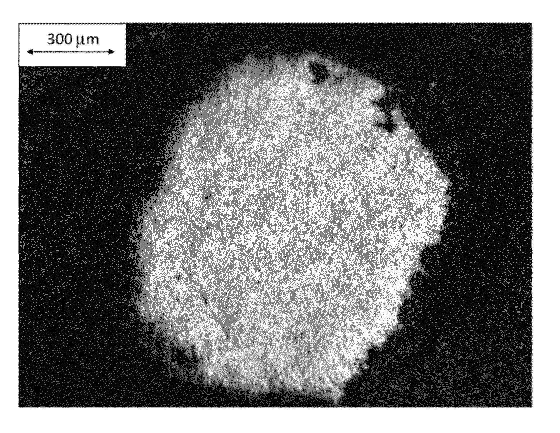
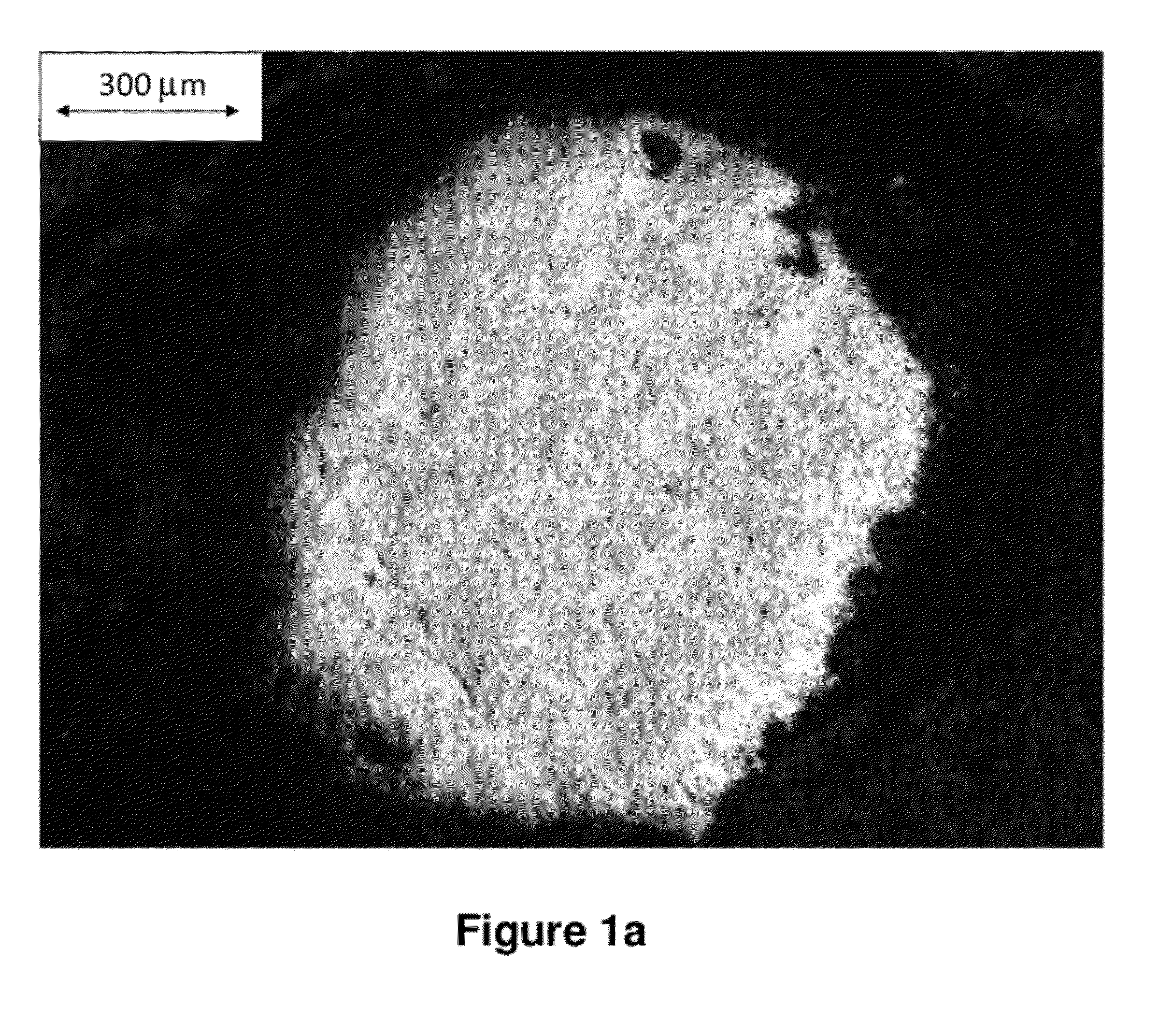
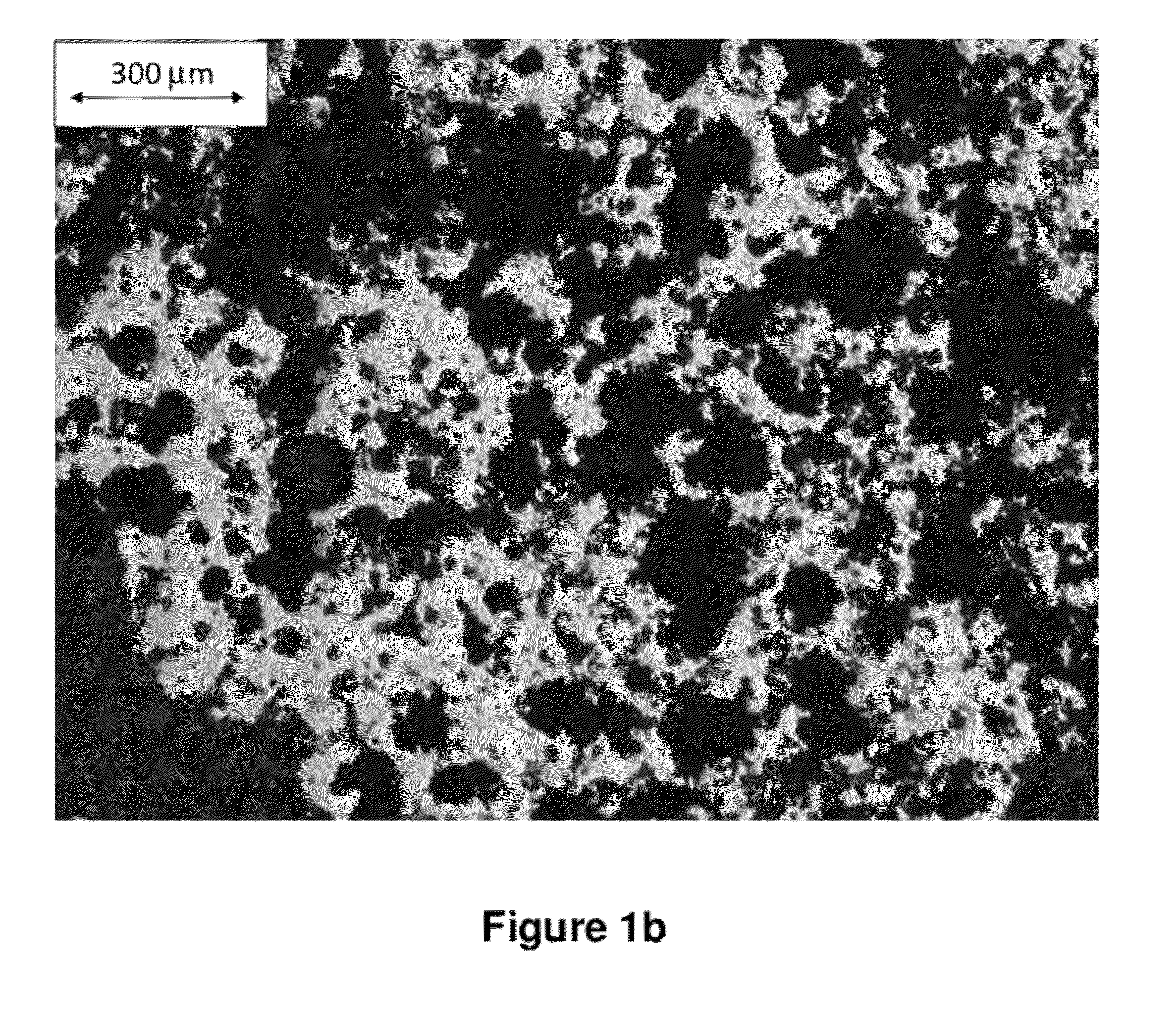
[0056]As required, embodiments of variable melting point solders of the present invention are disclosed herein. However, the disclosed embodiments are merely exemplary, and it should be understood that the invention may be embodied in many various and alternative forms. The Figures are not to scale and some features may be exaggerated or minimized to show details of particular elements while related elements may have been eliminated to prevent obscuring novel aspects.

[0057]Therefore, specific structural and functional details disclosed herein are not to be interpreted as limiting but merely as a basis for the claims and as a representative basis for teaching one skilled in the art to variously employ the present invention. For purposes of teaching and not limitation, the illustrated embodiments are directed to a solder based on a ternary or quaternary system of elements, comprising one or a combination of nickel (Ni) and antimony (Sb), combined with bismuth (Bi) and tin (Sn).

[0058]A...


PUM

PropertyMeasurementUnit
solidus temperatureaaaaaaaaaa

Abstract

The present invention relates to variable melting point solder formulations. The solder is comprised of at least one base metal or base metal alloy, preferably alloyed with at least one melting point depressant metal, such that the solidus point of the solder composition is reduced to an initial solidus temperature. Said base metal or base metal alloy, alloyed with at least one melting point depressant metal is mixed with at least one additive metal or additive metal alloy. When heated to a process temperature above said initial solidus temperature, a reaction occurs between the melting point depressant metal, and the additive metal, such that solidification occurs at the process temperature via the formation of intermetallic phases, effectively increasing the solidus of the base metal, and of the overall solder.

Description

CROSS REFERENCE TO RELATED U.S APPLICATION[0001]This patent application relates to, and claims the priority benefit from, U.S. Provisional Patent Application Ser. No. 61 / 377,302 filed on Aug. 26, 2010, entitled “VARIABLE MELTING POINT SOLDERS” which is incorporated herein by reference in its entirety.FIELD OF THE INVENTION[0002]This invention relates to solder materials, and more specifically variable melting point (VMP) solders.BACKGROUND OF THE INVENTION[0003]Solders are typically used in the microelectronics industry to join microelectronic circuit elements and packages (die, wafer, chip, etc) to each other and / or onto a circuit board. A solder may be present as a paste, as a metallization, metal layer or metal coating onto one or more joining surfaces, or as preforms placed upon the surfaces to be joined. These metalized surfaces or preforms may be used in a fluxless process such as thermo-compression bonding, or in conjunction with a chemical flux to promote melting, wetting, a...

Claims


Application Information

Patent Timeline
Patent Type & Authority Patents(United States)
IPC IPC(8): B23K35/26B23K1/00B23K31/02
CPCB23K35/262B23K1/0008B23K31/02B23K35/26B23K35/264
Inventor MCISAAC, DOUGLAS J.WHITNEY, MARK A.CORBIN, STEPHEN F.
Owner DYNAJOIN CORP
Why Eureka
Try Eureka