

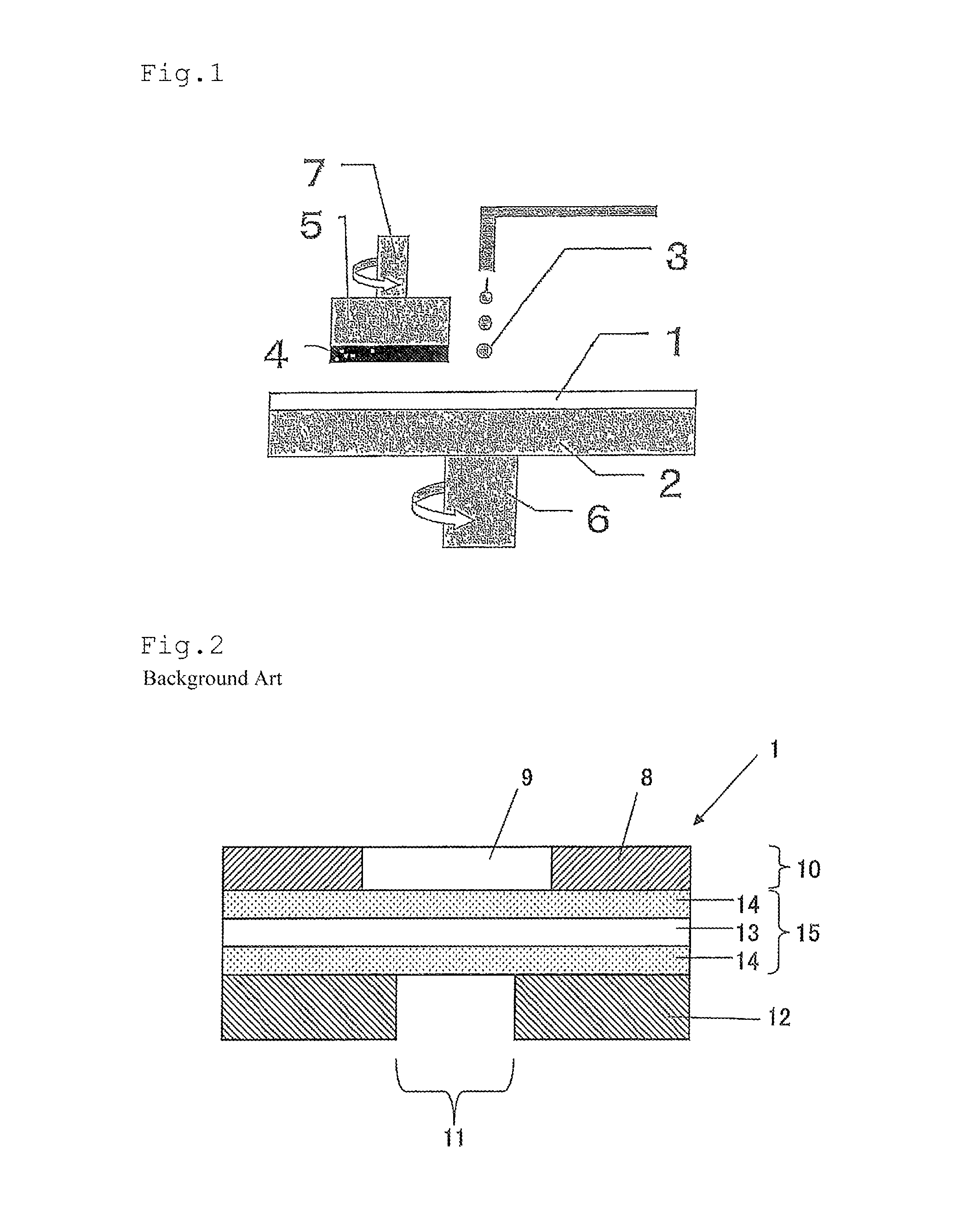
Polishing pad
a technology of polishing pad and surface, which is applied in the direction of lapping tools, electrical equipment, metal-working equipment, etc., can solve the problems of difficult prediction of processing results, waste of treatment time of test wafer, and inability to judge the planarity of the surface of the wafer, so as to prevent slurry leakage and high-accuracy optical end-point detection
- Summary
- Abstract
- Description
- Claims
- Application Information
AI Technical Summary
Benefits of technology
Problems solved by technology
Method used
Image

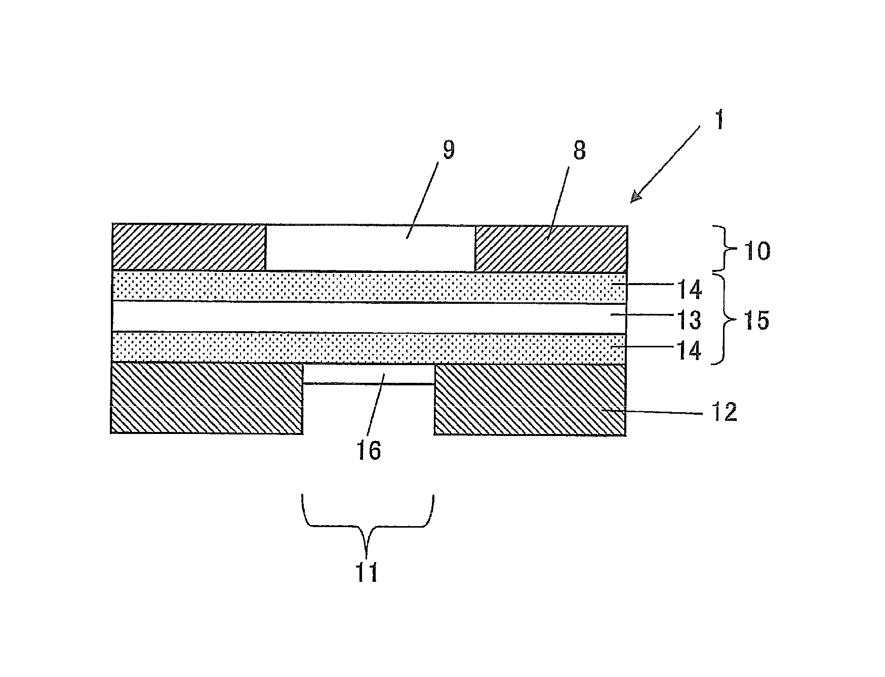
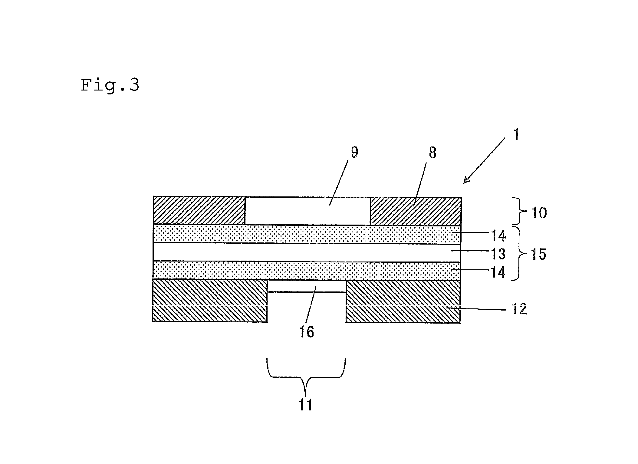
Examples
example 1
Preparation of Light-Transmitting Region
[0093]Polyester polyol (having a number average molecular weight of 2,400) (128 parts by weight) made of adipic acid, hexanediol and ethylene glycol was mixed with 30 parts by weight of 1,4-butanediol, and then the temperature of the mixed solution was controlled to 70° C. To this mixed solution, 100 parts by weight of 4,4′-diphenylmethane diisocyanate controlled to the temperature of 70° C. in advance, followed by stirring for about 1 minute. Then, the mixed solution was poured into a vessel maintained at 100° C. and post curing was carried out at 100° C. for 8 hours to prepare a polyurethane resin. Using the prepared polyurethane resin, a light-transmitting region (measuring 56 mm in length, 20 mm in width, and 1.25 mm in thickness) was prepared by injection molding.
[Preparation of Polishing Region]
[0094]In a reaction vessel, 100 parts by weight of a polyether-based prepolymer (Adiprene L-325, manufactured by Uniroyal Chemical Corporation, w...
example 2
Preparation of Polishing Pad
[0098]A release film on one surface of a double-sided tape including a release film (having a thickness of 38 μm) made of polyethylene terephthalate on both surfaces (a double tack tape, manufactured by Sekisui Chemical Co., Ltd.) was released, thereby exposing an adhesive layer. Using a laminator, the adhesive layer was stuck to a surface on the other side of the recessed surface of the polishing region prepared in Example 1 to prepare a polishing region attached with a double-sided tape. The light-transmitting region prepared in Example 1 was stuck to the adhesive layer in the opening of the polishing region attached with a double-sided tape to prepare a polishing layer attached with a double-sided tape. Thereafter, a transparent member (measuring 50 mm×14 mm) was formed by making a cut at the portion corresponding to the light-transmitting region of the release film of the other surface of the double-sided tape using a Thomson blade, thereby releasing ...
example 3
[0101]In the same manner as in Example 1, except that an anti-reflection film (REALOOK, manufactured by NOF Corporation) was used as the transparent member, a polishing pad was prepared.
PUM
 Abstract
Description
Claims
Application Information