Methods of forming embedded resistors for resistive random access memory cells

a random access memory and embedded resistor technology, applied in the direction of basic electric elements, electrical equipment, semiconductor devices, etc., can solve the problems of over-programming, over-current through the resistive switching layer, and consuming more power than fewer, so as to achieve the effect of reducing the number of resistive switching layers

Active Publication Date: 2015-09-22
INTERMOLECULAR
View PDF11 Cites 187 Cited by
  • Summary
  • Abstract
  • Description
  • Claims
  • Application Information

AI Technical Summary

Benefits of technology

[0004]Provided are memory cells including resistive switching layers having silicon, oxygen, and nitrogen as well as embedded resistor layers having a metal, silicon, and nitrogen. In some embodiments, silicon may be partially or completely replaced with aluminum. The embedded resistor may also have oxygen. A resistive switching layer directly interfaces an embedded resistor layer of the same cell. A portion of each layer forming this interface may be formed substantially of silicon nitride and may be formed in the same deposition chamber without breaking vacuum. For example, these portions may be formed by sequential atomic layer deposition cycles. However, silicon concentrations in these portions may be different. Specifically, the silicon concentration of the embedded resistor portion may be less than the silicon concentration of the resistive switching layer portion. This variation may be achieved by varying one or more process conditions during fabrication of the memory cell.

Problems solved by technology

For example, when the resistive switching layer is switched from its high resistive state (HRS) to its low resistive state (LRS), a rapid drop in resistance associated with this switch may cause an excessive current through the resistive switching layer and an over-programming.
However, shorter pulses have their own inherent limitations, such as requiring more pulses or higher voltages to achieve the same switching result, which may consume more power than fewer, longer, lower-voltage pulses.
Furthermore, even during a relatively short switching pulse, the change in resistance may be sufficiently large to result in current spiking and over-programming.
That is, defects may travel through an interface formed by this electrode with the resistive switching layer (i.e., the reactive interface).
Furthermore, there may be some mobility of defects within resistive switching layer 104.
This breakage generally does not correspond to complete dispersion of defects forming these conductive paths and may be a self-limiting process, i.e., the process may stop after some initial breakage occurs.

Method used


Image

  • Methods of forming embedded resistors for resistive random access memory cells
  • Methods of forming embedded resistors for resistive random access memory cells
  • Methods of forming embedded resistors for resistive random access memory cells

Examples


Embodiment Construction

[0025]A detailed description of various embodiments is provided below along with accompanying figures. The detailed description is provided in connection with such embodiments, but is not limited to any particular example. The scope is limited only by the claims and numerous alternatives, modifications, and equivalents are encompassed. Numerous specific details are set forth in the following description in order to provide a thorough understanding. These details are provided for the purpose of example and the described techniques may be practiced according to the claims without some or all of these specific details. For the purpose of clarity, technical material that is known in the technical fields related to the embodiments has not been described in detail to avoid unnecessarily obscuring the description.

INTRODUCTION

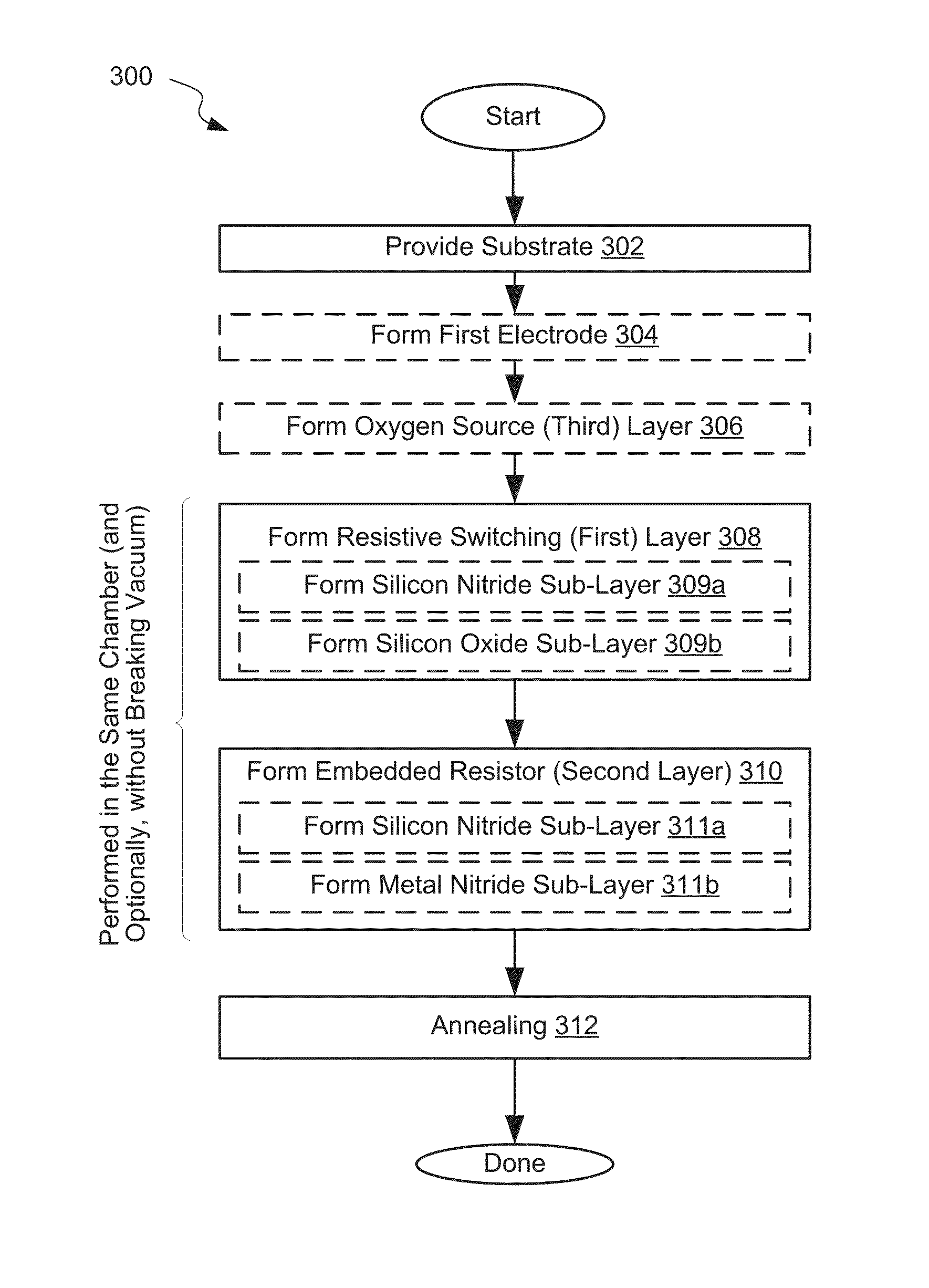
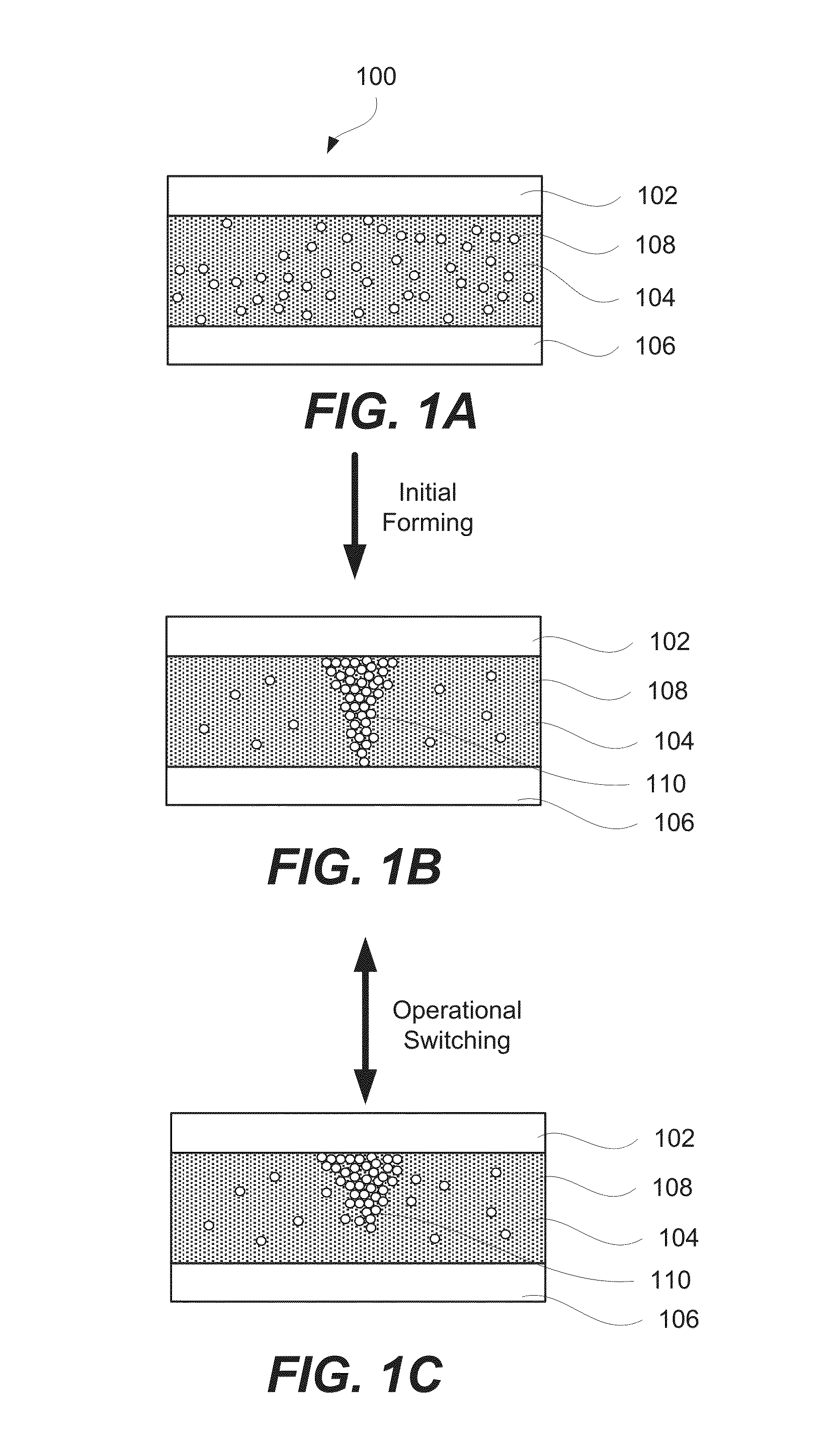
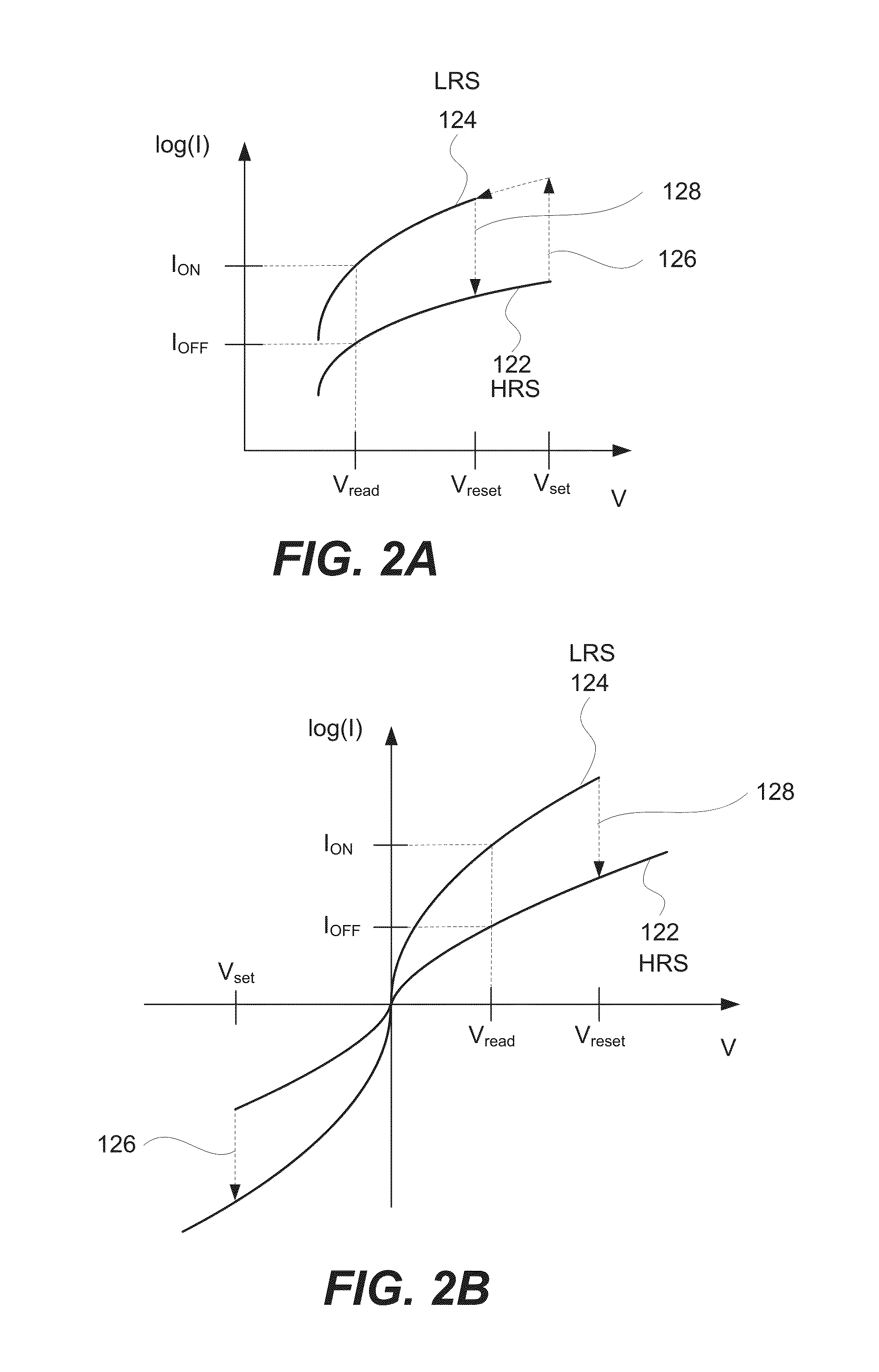
[0026]A ReRAM cell exhibiting resistive switching characteristics generally includes multiple layers formed into a stack, such as a “metal-insulator-metal” (MIM) stack...


PUM


Abstract

Provided are memory cells including resistive switching layers having silicon, oxygen, and nitrogen as well as embedded resistor layers having a metal, silicon, and nitrogen. In some embodiments, silicon may be partially or completely replaced with aluminum. The embedded resistor may also have oxygen. A resistive switching layer directly interfaces an embedded resistor layer of the same cell. A portion of each layer forming this interface may be formed substantially of silicon nitride and may be formed in the same deposition chamber without breaking vacuum. For example, these portions may be formed by sequential atomic layer deposition cycles. However, silicon concentrations in these portions may be different. Specifically, the silicon concentration of the embedded resistor portion may be less than the silicon concentration of the resistive switching layer portion. This variation may be achieved by varying one or more process conditions during fabrication of the memory cell.

Description

BACKGROUND[0001]Nonvolatile memory is computer memory capable of retaining stored information even when unpowered. Non-volatile memory is typically used for secondary storage or long-term persistent storage and may be used in addition to volatile memory, which loses the stored information when unpowered. Nonvolatile memory can be permanently integrated into computer systems (e.g., solid state hard drives) or can take the form of removable and easily transportable memory cards (e.g., USB flash drives). Nonvolatile memory is becoming more popular because of its small size / high density, low power consumption, fast read and write rates, retention, and other characteristics.[0002]Flash memory is a common type of nonvolatile memory because of its high density and low fabrication costs. Flash memory is a transistor-based memory device that uses multiple gates per transistor and quantum tunneling for storing the information on its memory device. Flash memory uses a block-access architecture...

Claims


Application Information

Patent Timeline
Patent Type & Authority Patents(United States)
IPC IPC(8): H01L29/02H01L45/00
CPCH01L45/06H01L45/1625H10B63/20H10B63/84H10N70/24H10N70/801H10N70/826H10N70/883H10N70/023H10N70/011H10N70/231H10N70/026
Inventor WANG, YUN
Owner INTERMOLECULAR
Why Eureka
Try Eureka