Nitride semiconductor structure and semiconductor light emitting device including the same

a technology of nitride and semiconductor, applied in the direction of semiconductor devices, basic electric elements, electrical equipment, etc., can solve the problems of light emission, low light extraction rate, and first method only being used to treat an exposed p-type gan semiconductor layer on top of the led chip, so as to improve the recombination rate of electrons, increase light emission efficiency, and strengthen coupling

Active Publication Date: 2015-09-29
GENESIS PHOTONICS
View PDF6 Cites 4 Cited by
  • Summary
  • Abstract
  • Description
  • Claims
  • Application Information

AI Technical Summary

Benefits of technology

[0008]Therefore it is a primary object of the present invention to provide a nitride semiconductor structure in which a second type doped semiconductor layer has a high concentration of a second type dopant (larger than 5×1019 cm−3) and a thickness that is smaller than 30 nm so as to improve the light-extraction efficiency.
[0009]It is another object of the present invention to provide a semiconductor light emitting device including the above nitride semiconductor structure for providing a good light emitting efficiency.
[0011]Moreover, a hole supply layer is disposed between the light emitting layer and the second type doped semiconductor layer. The hole supply layer is made of AlxInyGa1-x-yN while x and y satisfy the conditions: 0<x<1, 0<y<1, and 0<x+y<1. The hole supply layer is doped with a second type dopant at a concentration larger than 1018 cm−3. The hole supply layer is also doped with a Group IV-A element at a concentration ranging from 1017 cm−3 to 1020 cm−3 so that more holes are provided to enter the light emitting layer and the electron-hole recombination is further increased. The light emitting layer has a multiple quantum well (MQW) structure. The band gap of the hole supply layer is larger than that of the well layer of the MQW structure so that holes in the hole supply layer can enter the well layer of the MQW structure. Thus the electron-hole recombination rate is increased and the light emitting efficiency is further improved.
[0013]Furthermore, a second type carrier blocking layer made of AlxGa1-xN (0<x<1) is disposed between the hole supply layer and the second type doped semiconductor layer while a first type carrier blocking layer made of AlxGa1-xN (0<x<1) is disposed between the light emitting layer and the first type doped semiconductor layer. Due to the property that the band gap of AlGaN containing aluminum is larger than the band gap of GaN, carriers are confined in the MQW structure and electron-hole recombination rate is improved. Thus the light emitting efficiency is increased.
[0014]A semiconductor light emitting device of the present invention includes the above nitride semiconductor structure disposed on a substrate, a first type electrode and the second type electrode used together for providing electric power. Due to smaller thickness of the second type doped semiconductor layer, the second type electrode is getting closer to the surface of the light emitting layer. Thus a stronger coupling is generated due to resonance between photons from the light emitting layer and surface plasmon. Therefore the light emitting efficiency is improved. Moreover, the second type doped semiconductor layer has a higher concentration of the second type dopant than that of the conventional p-type GaN layer so that the resistance of the second type doped semiconductor layer is lower. Thus even current spreading in the second type doped semiconductor layer is achieved when the current flows from the second type electrode to the first type electrode. Therefore the LED gets a better light emitting efficiency.

Problems solved by technology

Due to total internal reflection of GaN and air, light emitting from LED is restricted inside the LED and the light-extraction rate is quite low.
However, the first method can only be used to treat an exposed p-type GaN semiconductor layer on top of the LED chip.
Thus the improvement of the light-extraction efficiency has a certain limit.
The process of the second method is quite complicated and the glue has a problem of poor heat dissipation.
Therefore the light emitting efficiency of LED produced by the above two methods is unable to be increased effectively.
Moreover, the concentration of the dopant in the p-type GaN layer is unable to be increased effectively so that the resistance of the p-type GaN layer is quite large.
Thus current is unable to be spread evenly in the p-type GaN layer when the current flows from metal electrodes to the GaN semiconductor layer.

Method used


Image

  • Nitride semiconductor structure and semiconductor light emitting device including the same
  • Nitride semiconductor structure and semiconductor light emitting device including the same
  • Nitride semiconductor structure and semiconductor light emitting device including the same

Examples


Embodiment Construction

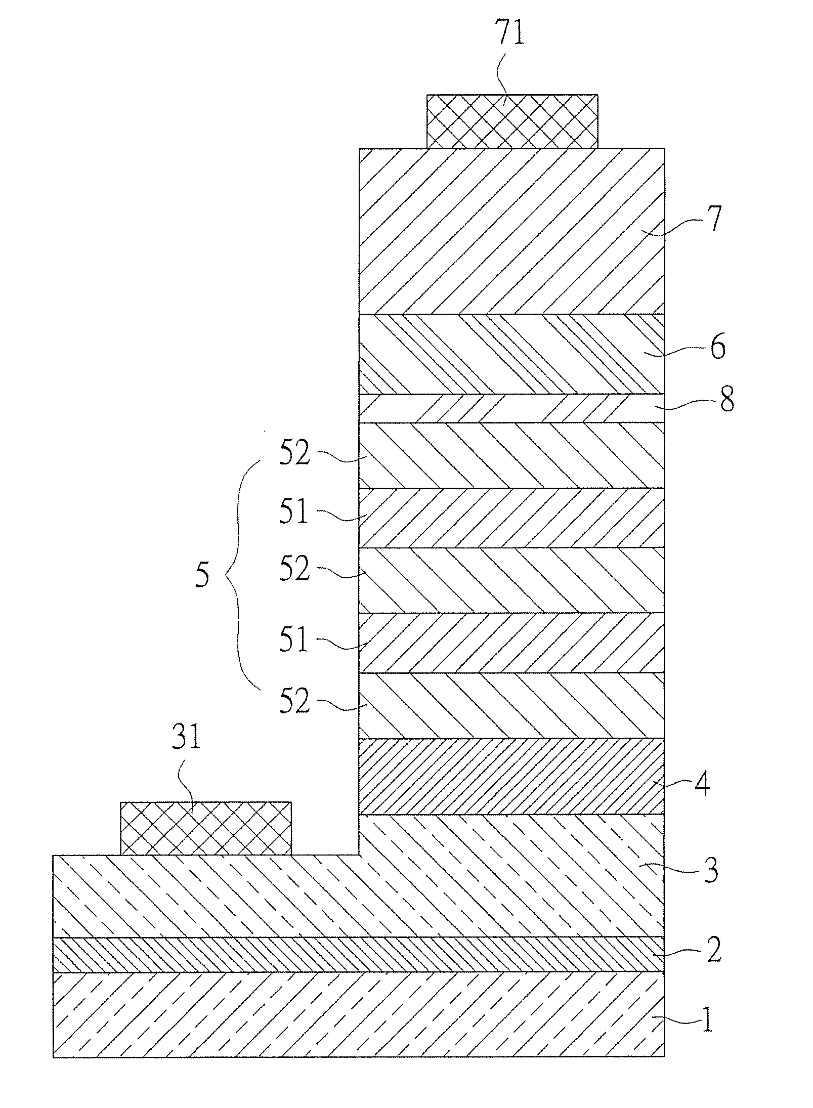
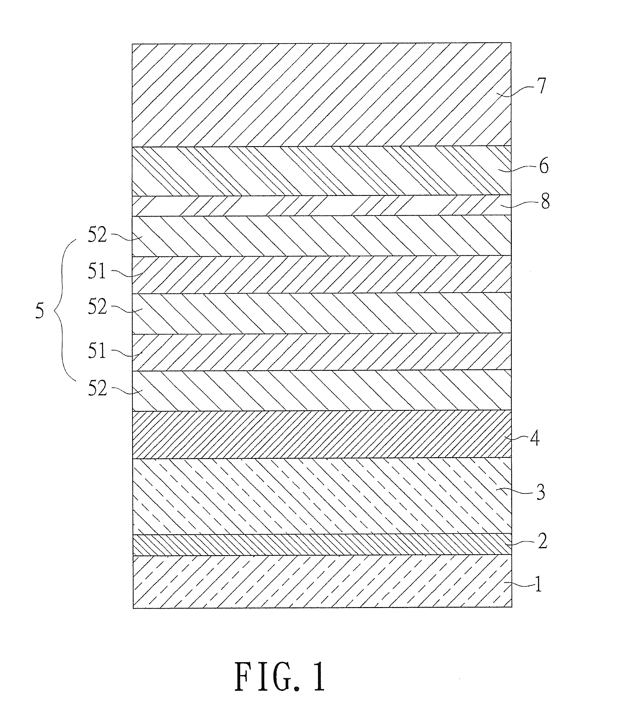
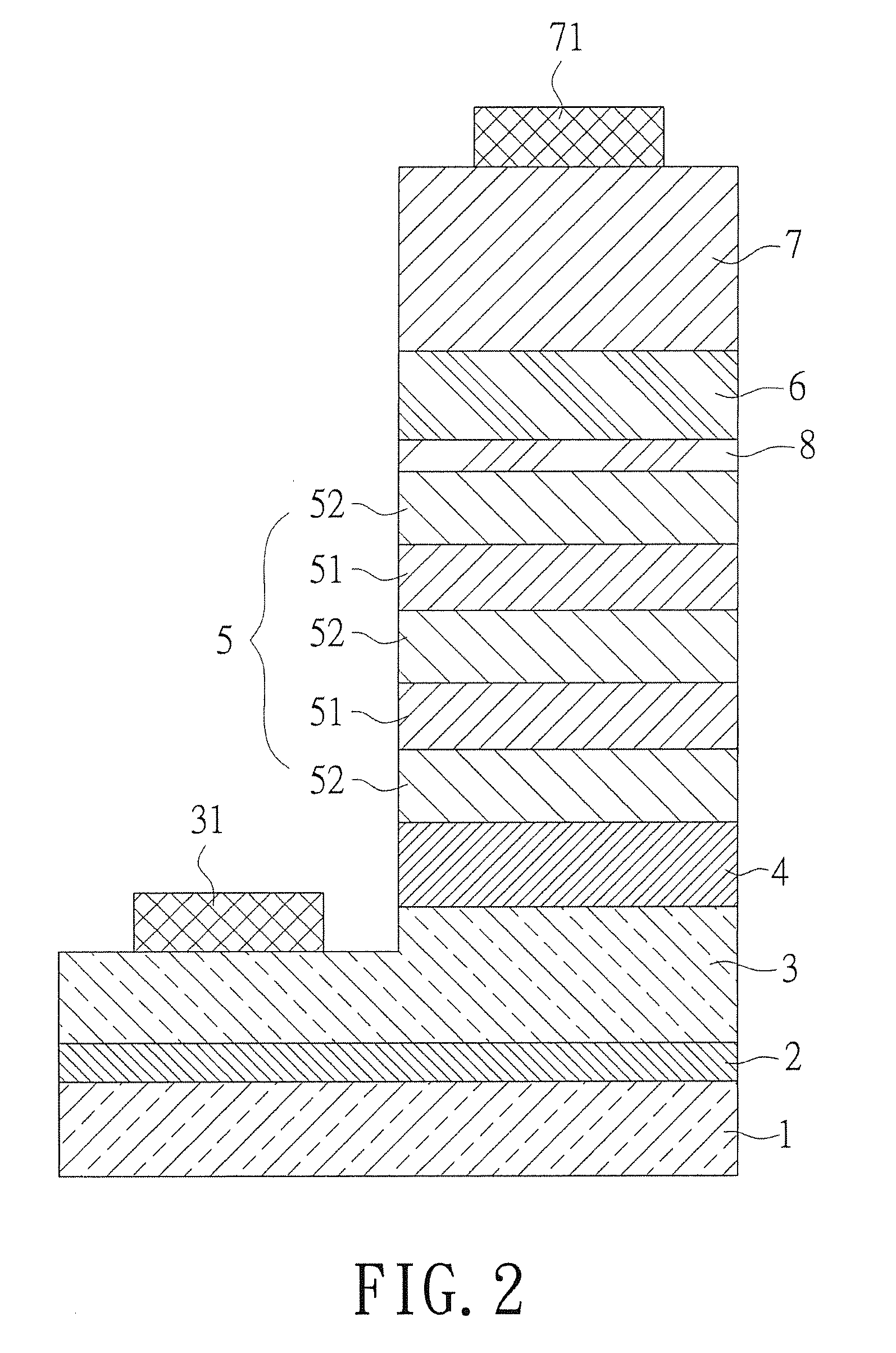
[0018]In the following embodiments, when it is mentioned that a layer of something or a structure is disposed over or under a substrate, another layer of something, or another structure, that means the two structures, the layers of something, the layer of something and the substrate, or the structure and the substrate can be directly or indirectly connected. The indirect connection means there is at least one intermediate layer disposed therebetween.

[0019]Referring to FIG. 1, a cross section of an embodiment of nitride semiconductor structure according to the present invention is revealed. The nitride semiconductor structure includes a first type doped semiconductor layer 3 and a second type doped semiconductor layer 7. A light emitting layer 5 is disposed between the first type doped semiconductor layer 3 and the second type doped semiconductor layer 7. The second type doped semiconductor layer 7 is doped with a second type dopant at a concentration larger than 5×1019 cm−3 while a ...


PUM


Abstract

A nitride semiconductor structure and a semiconductor light emitting device are revealed. The semiconductor light emitting device includes a substrate disposed with a first type doped semiconductor layer and a second type doped semiconductor layer. A light emitting layer is disposed between the first type doped semiconductor layer and the second type doped semiconductor layer. The second type doped semiconductor layer is doped with a second type dopant at a concentration larger than 5×1019 cm−3 while a thickness of the second type doped semiconductor layer is smaller than 30 nm. Thereby the semiconductor light emitting device provides a better light emitting efficiency.

Description

BACKGROUND OF THE INVENTION[0001]1. Field of the Invention[0002]The present invention relates to a nitride semiconductor structure and a semiconductor light emitting device, especially to a nitride semiconductor structure and a semiconductor light emitting device including a second type doped semiconductor layer with a high dopant concentration (larger than 5×1019 cm−3) and a small thickness (smaller than 30 nm) to improve a light-extraction efficiency and make the semiconductor light emitting device have a better light emitting efficiency.[0003]2. Description of Related Art[0004]Generally, a nitride light emitting diode is produced by forming a buffer layer on a substrate first. Then a n-type semiconductor layer, a light emitting layer and a p-type semiconductor layer are formed on the buffer layer in turn by epitaxial growth. Next use photolithography and etching processes to remove a part of the p-type semiconductor layer and a part of the light emitting layer until a part of the...

Claims


Application Information

Patent Timeline
Patent Type & Authority Patents(United States)
IPC IPC(8): H01L29/06H01L33/06H01L33/14H01L33/32
CPCH01L33/06H01L33/14H01L33/32H01L33/0025H01L33/325
Inventor LAI, YEN-LINWU, JYUN-DELI, YU-CHU
Owner GENESIS PHOTONICS
Why Eureka
Try Eureka