Transferable probe tips

a technology of probe tips and transferable tips, which is applied in the direction of mechanical roughness/irregularity measurement, semiconductor/solid-state device testing/measurement, instruments, etc., can solve the problems of scalability, material selection flexibility, cost of fabrication, and difficulty in achieving the effect of existing approaches

Active Publication Date: 2015-12-01
INT BUSINESS MASCH CORP
View PDF22 Cites 5 Cited by
  • Summary
  • Abstract
  • Description
  • Claims
  • Application Information

AI Technical Summary

Problems solved by technology

The scaling of wafer probes to finer pitch presents challenges, as the cost and complexity of wafer probe technology increases.
By way of example, in existing approaches, challenges in probe tips include scalability, material selection flexibility, and cost of fabrication.
However, there is demand for probing solutions for area array pitches 50 microns and smaller, solutions which are difficult to achieve with existing approaches.

Method used


Image

  • Transferable probe tips
  • Transferable probe tips
  • Transferable probe tips

Examples


Embodiment Construction

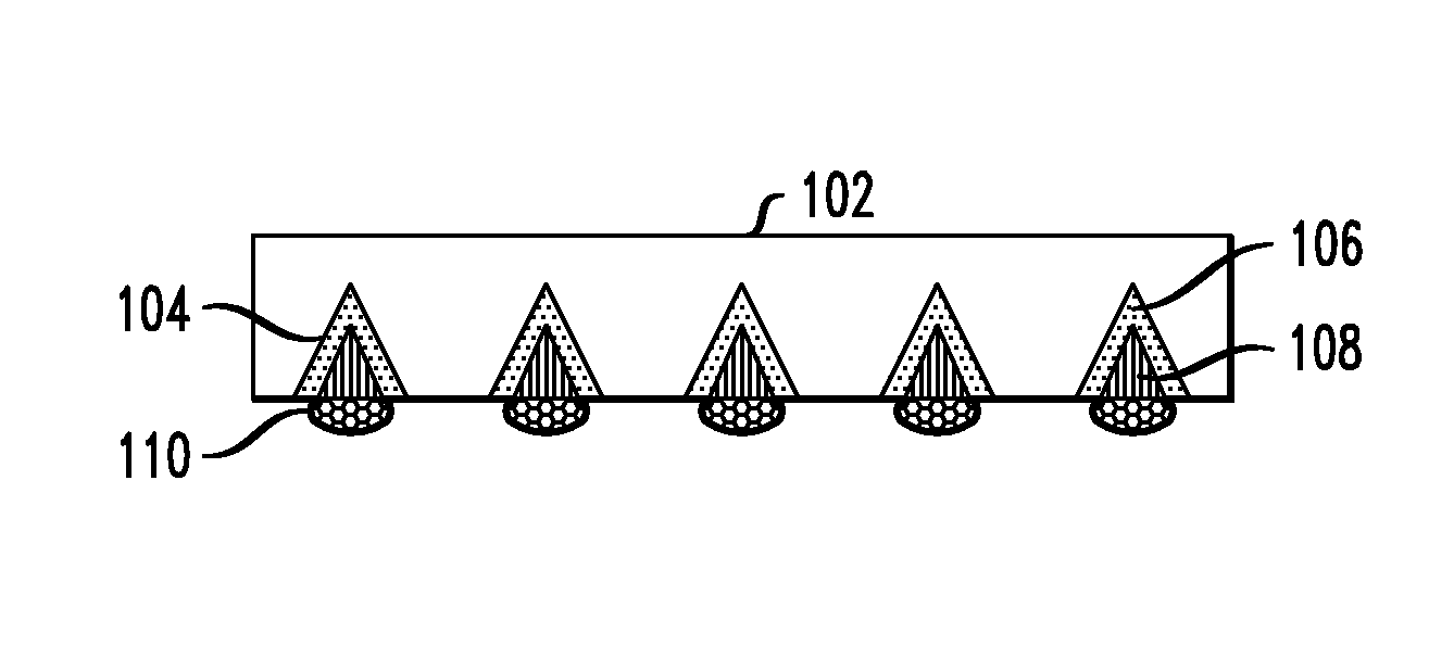
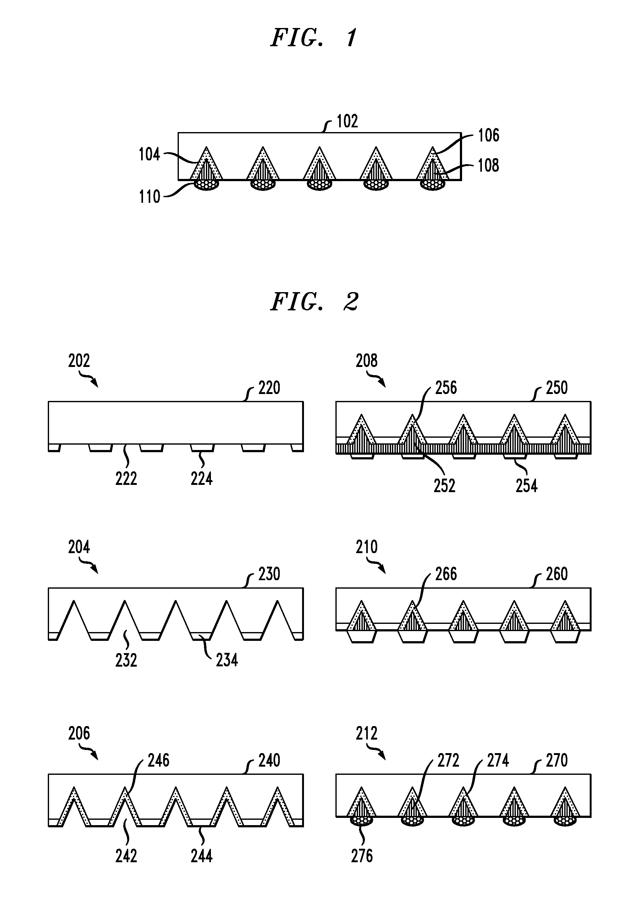
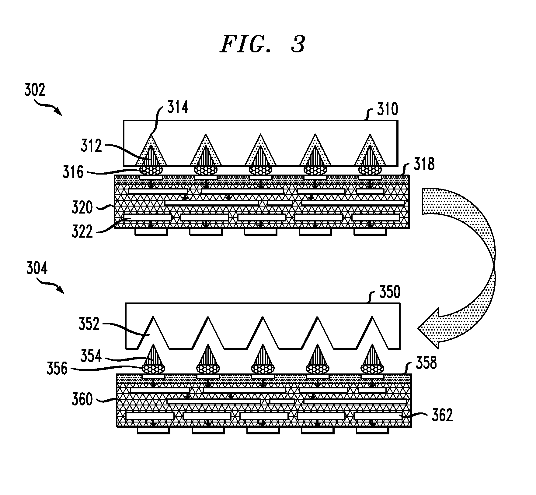
[0014]Principles of the present invention include techniques for the fabrication and transfer of fine-pitch probe tips. As detailed herein, fine-pitch probe arrays can be pre-fabricated in a temporary handler substrate. The handler substrate can then be flip-chip joined to a target probe head substrate (such as, for example, a probe card or test interposer) to transfer the probe arrays.

[0015]As described herein, one or more embodiments of the invention can include one of two ways to remove a structure on top of a delamination layer (that is, a low-adhesion or sacrificial layer): 1) rely on a very low-adhesion layer, which allows the structure to be pealed off (essentially a mechanical delamination process), or 2) provide a layer (for example, a sacrificial layer) that either thermally decomposes or can be chemically dissolved, which also allows delamination.

[0016]As used herein, a handler substrate refers to a silicon substrate used to fabricate and handle transferable probe tips, a...


PUM

PropertyMeasurementUnit
metallicaaaaaaaaaa
adhesionaaaaaaaaaa
anisotropicaaaaaaaaaa

Abstract

Transferable probe tips including a metallic probe, a delamination layer covering a portion of the metallic probe, and a bonding alloy, wherein the bonding alloy contacts the metallic probe at a portion of the probe that is not covered by the delamination layer are provided herein. Also, techniques for creating a transferable probe tip are provided, including etching a handler substrate to form one or more via arrays, depositing a delamination layer in each via array, depositing one or more metals in each via array to form a probe tip structure, and depositing a bonding alloy on a portion of the probe tip structure that is not covered by the delamination layer. Additionally, techniques for transferring transferable probe tips are provided, including removing a handler substrate from a probe tip structure, and transferring the probe tip structure via flip-chip joining the probe tip structure to a target probe head substrate.

Description

FIELD OF THE INVENTION[0001]The present invention generally relates to probe-based technologies, and, more particularly, to probe tips.BACKGROUND OF THE INVENTION[0002]The scaling of wafer probes to finer pitch presents challenges, as the cost and complexity of wafer probe technology increases. By way of example, in existing approaches, challenges in probe tips include scalability, material selection flexibility, and cost of fabrication. Conventional probe card and probe tip technologies have been extended to cover area array interconnection pitches down to the range 150-200 microns. However, there is demand for probing solutions for area array pitches 50 microns and smaller, solutions which are difficult to achieve with existing approaches. Furthermore, there is a need for fine-pitch probing solutions for three-dimensional silicon device structures.SUMMARY OF THE INVENTION[0003]Principles of the present invention provide transferable probe tips. In one example embodiment of the inv...

Claims


Application Information

Patent Timeline
Patent Type & Authority Patents(United States)
IPC IPC(8): G01N27/84H01L21/66H01L21/44G01R31/26G01R33/12G01B5/28G01R3/00G01R1/073G03F7/00G01Q40/02G01Q70/16G01R1/067G01Q70/14
CPCG01B5/28G01R1/07378G01R3/00G03F7/00G01R1/06738G01Q70/14G01Q70/16G01R1/067G01Q40/02B81C3/001B81B2201/12B81C2201/0194
Inventor ANDRY, PAUL S.DANG, BINGWRIGHT, STEVEN L.
Owner INT BUSINESS MASCH CORP
Why Eureka
Try Eureka