
Passive waveguide structure with alternating GaInAs/AlInAs layers for mid-infrared optoelectronic devices

a passive waveguide and gainas/alinas technology, applied in semiconductor lasers, laser details, electrical devices, etc., can solve the problems of bulky and expensive, and achieve the effect of large band gaps

Active Publication Date: 2016-01-05
THORLABS QUANTUM ELECTRONICS
View PDF8 Cites 2 Cited by
  • Summary
  • Abstract
  • Description
  • Claims
  • Application Information

AI Technical Summary

Benefits of technology

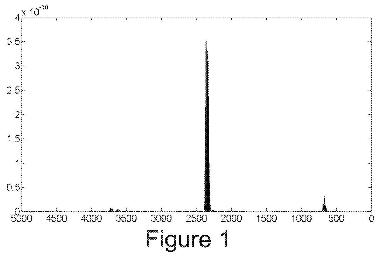
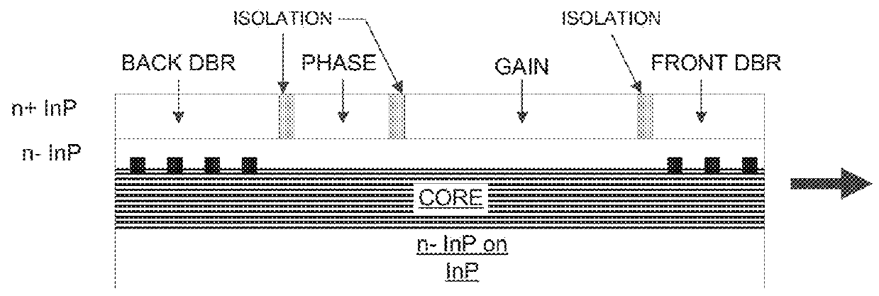
[0010]To provide the benefits described above of including in a DBR QCL a transparent waveguide as well as to provide for similar benefits of a transparent waveguide in other semiconductor active optical devices, the present disclosure includes a transparent (or relatively transparent) waveguide structure made of two alternating layers of semiconductor materials A and B, which have refractive indexes of Na and Nb. Desirably, at least one of A and B should have a relatively large band gap so that the passive waveguide structure can block electric current very well, even under relatively high voltage bias. The effective index of the optical mode in the passive waveguide No will be in-between Na and Nb; for good propagation of the optical mode, No should be equal (or close) to the refractive index in an associated gain section which is butt-jointed with the passive waveguide. Also for good propagation of the optical mode, the size of the optical mode(s) in the passive and gain section should be equal or reasonably so.

Problems solved by technology

External cavity QCLs can have both single wavelength emission and wide tuning range, but they are usually expensive and bulky.

Method used


Image

  • Passive waveguide structure with alternating GaInAs/AlInAs layers for mid-infrared optoelectronic devices
  • Passive waveguide structure with alternating GaInAs/AlInAs layers for mid-infrared optoelectronic devices
  • Passive waveguide structure with alternating GaInAs/AlInAs layers for mid-infrared optoelectronic devices

Examples


Embodiment Construction

[0020]The present invention can be understood more readily by reference to the following detailed description, drawings, examples, and claims, and their previous and following description. However, before the present compositions, articles, devices, and methods are disclosed and described, it is to be understood that this invention is not limited to the specific compositions, articles, devices, and methods disclosed unless otherwise specified, as such can, of course, vary. It is also to be understood that the terminology used herein is for the purpose of describing particular aspects only and is not intended to be limiting.

[0021]The following description of the invention is provided as an enabling teaching of the invention in its currently known embodiments. To this end, those skilled in the relevant art will recognize and appreciate that many changes can be made to the various aspects of the invention described herein, while still obtaining the beneficial results of the present inv...


PUM


Abstract

Disclosed is a semiconductor optical emitter having an optical mode and a gain section, the emitter comprising a low loss waveguide structure made of two alternating layers of semiconductor materials A and B, having refractive indexes of Na and Nb, respectively, with an effective index No of the optical mode in the low loss waveguide between Na and Nb, wherein No is within a 5% error margin of identical to a refractive index of the gain section and wherein the gain section is butt-jointed with the low loss waveguide, and wherein the size and shape of the optical mode(s) in the low loss waveguide and gain section are within a 10% error margin of equal. Desirably, at least one of the semiconductor materials A and B has a sufficiently large band gap that the passive waveguide structure blocks current under a voltage bias of 15 V.

Description

CROSS-REFERENCE TO RELATED APPLICATIONS[0001]This application claims the benefit of U.S. Provisional Patent Application No. 61 / 946,700 filed on Feb. 28, 2014. The disclosure of U.S. Provisional Patent Application No. 61 / 946,700 is hereby incorporated by reference.[0002]This application is also related to Provisional Application Ser. No. 61 / 732,289 filed on Nov. 30, 2012, and to Application No. PCT / US2013 / 072195 filed on Nov. 27, 2013.FIELD OF THE INVENTION[0003]The present specification generally relates to quantum cascade lasers (“QCLs”) and particularly to passive waveguide structures for use in QCLs and to QCLs using such structures.TECHNICAL BACKGROUND[0004]A quantum cascade laser is a unipolar device. It utilizes intersubband transitions, unlike the traditional direct band gap semiconductor lasers, and it usually emits in the mid-infrared (“mid-IR”) or far-infrared (“far-IR”) wavelength range.[0005]Mid-IR sources are of interest for various reasons. Strong absorption lines in t...

Claims


Application Information

Patent Timeline
Patent Type & Authority Patents(United States)
IPC IPC(8): H01S5/00H01S5/02H01S5/34H01S5/20H01S5/026
CPCH01S5/026H01S5/0208H01S5/2031H01S5/3402H01S5/06256H01S5/2206H01S5/3401H01S2301/185
Inventor CANEAU, CATHERINE GENEVIEVEXIE, FENGZAH, CHUNG-EN
Owner THORLABS QUANTUM ELECTRONICS
Learn More