Pixel structure with data line, scan line and gate electrode formed on the same layer and manufacturing method thereof

a technology of pixel structure and data line, applied in the field of pixel structure, can solve the problems of increasing the load of data line and affecting display voltage, and achieve the effect of reducing the parasitic capacitance of pixel structure and reducing the electricity consumption of pixel structur

Active Publication Date: 2016-01-19
AU OPTRONICS CORP
View PDF13 Cites 9 Cited by
  • Summary
  • Abstract
  • Description
  • Claims
  • Application Information

AI Technical Summary

Benefits of technology

[0007]Accordingly, the present invention is directed to a pixel structure, which may reduce the parasitic capacitance of the pixel structure and further reduce the electricity consumption of the pixel structure.
[0008]The present invention is also directed to a method of manufacturing a pixel structure, which may simplify manufacturing process steps for reducing the number of photo masks to decrease the required cost.
[0011]Based on the above, in the pixel structure and the manufacturing method thereof according to the present invention, the linear transmitting part of the data line, the scan line and the gate electrode are formed on the same layer by patterning the first conductive layer, and the second insulating layer, located on the channel of the active device and used as the etching blocking layer, is further disposed on the linear transmitting part of the data line. In this case, when the common electrode manufactured via the second conductive layer overlaps with the linear transmitting part of the data line, multiple insulating layers are disposed between the linear transmitting part of the data line and the common electrode. In this way, the etching blocking pattern defined by the second insulating layer is used for protecting the channel, and the capacitive coupling effect between the data line and the common electrode is reduced by further disposing the second insulating layer between the linear transmitting part of the data line and the common electrode, so that the power consumption of the pixel structure is reduced.

Problems solved by technology

Due to the coupling effect between the pixel electrode and the data line, such design usually affects the display voltage of the pixel electrode.
The existence of the parasitic capacitance will increase the load of the data line, which is unfavourable to the driving of the thin film transistor array.

Method used


Image

  • Pixel structure with data line, scan line and gate electrode formed on the same layer and manufacturing method thereof
  • Pixel structure with data line, scan line and gate electrode formed on the same layer and manufacturing method thereof
  • Pixel structure with data line, scan line and gate electrode formed on the same layer and manufacturing method thereof

Examples


first embodiment

[0047

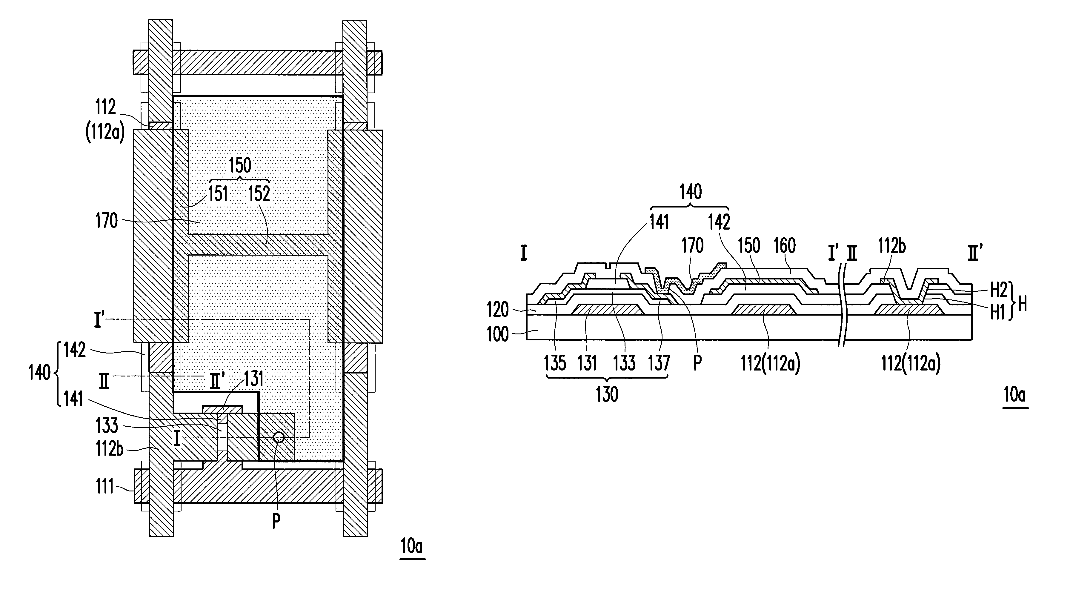
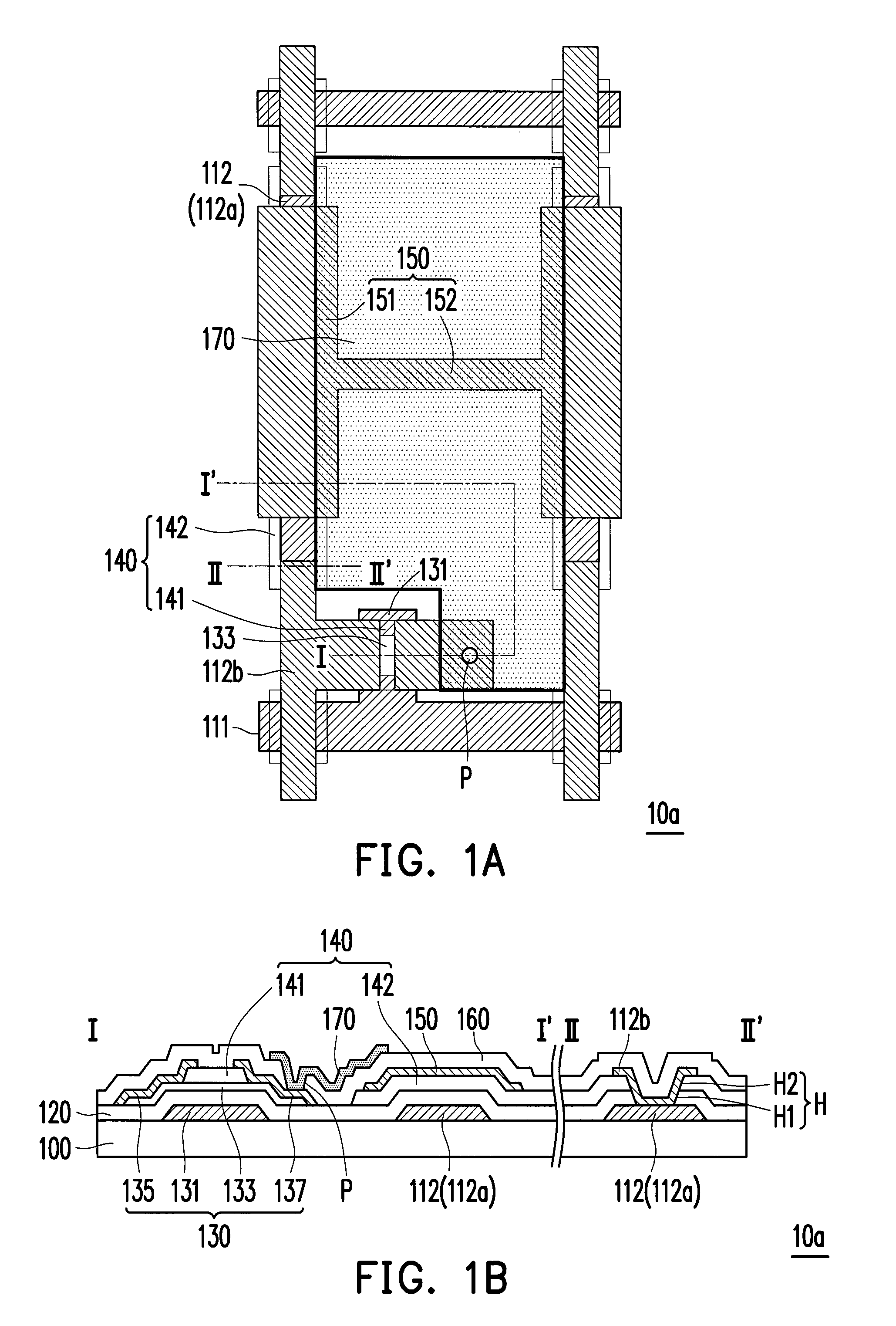
[0048]FIG. 1A is a schematic top view of a pixel structure of the first embodiment of the present invention, while FIG. 1B is a cross-sectional view of the pixel structure in FIG. 1A along section lines I-I′ and II-II′. Referring to FIG. 1A and FIG. 1B, the pixel structure 10a of this embodiment includes a substrate 100, a scan line 111, a data line 112, a first insulating layer 120, an active device 130, a second insulating layer 140, a common electrode 150 and a first pixel electrode 170. The active device includes a gate electrode 131, an oxide semiconductor layer (or named an oxide channel) 133, a source electrode 135 and a drain electrode 137.

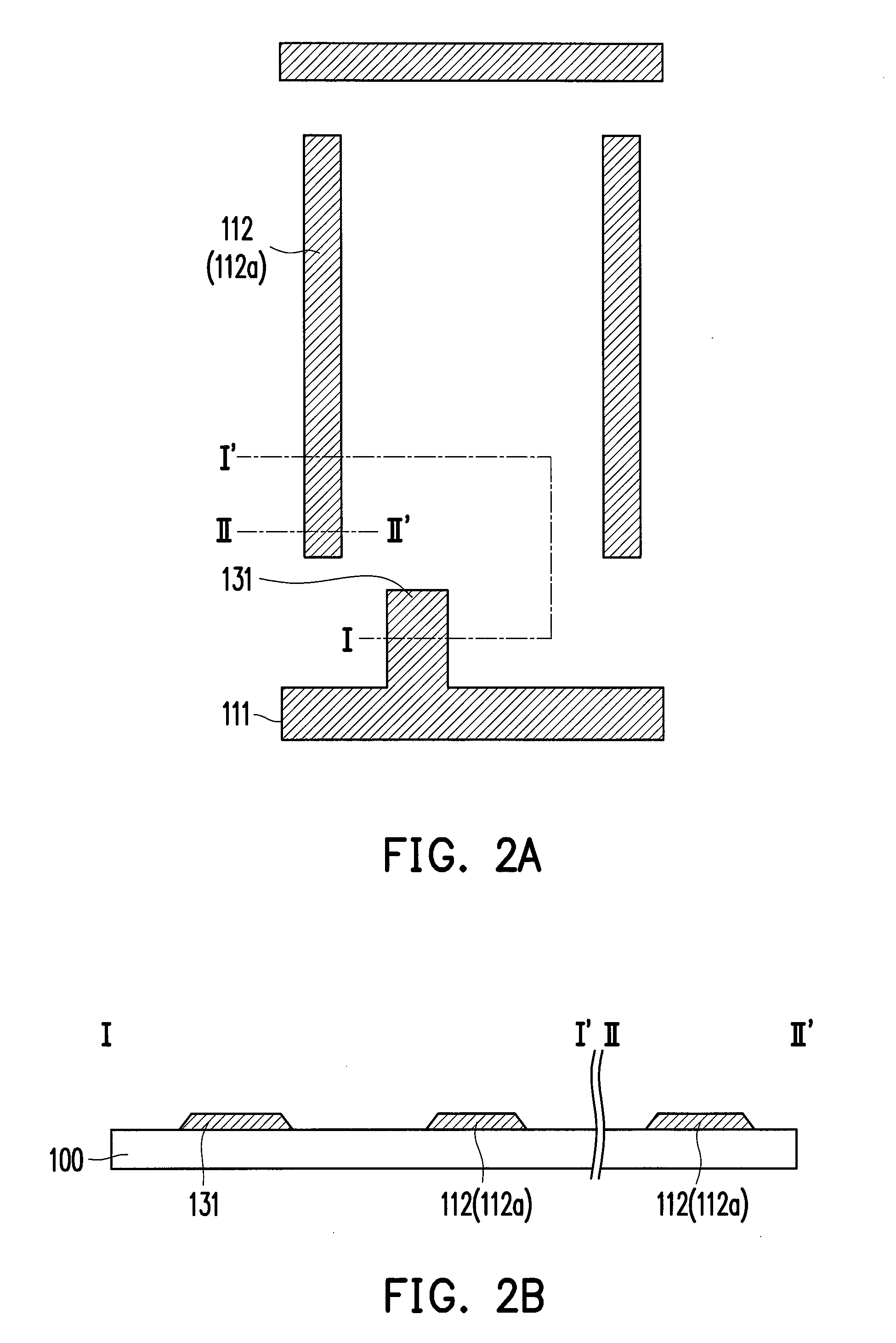
[0049]Specifically speaking, the scan line 111 is disposed on the substrate 100. The data line 112 is disposed on the substrate 100, the scan line 111 is crossed to the data line 112, and the data line 112 includes a linear transmitting part 112a and a cross-line transmitting part 112b connected to each other, where the cross-line tra...

second embodiment

[0064

[0065]FIG. 9A is a schematic top view of a pixel structure of the second embodiment of the present invention, while FIG. 9B is a cross-sectional view of the pixel structure in FIG. 9A along section lines III-III′ and IV-IV′. Referring to FIG. 9A and FIG. 9B, the pixel structure 10b in this embodiment is similar to the pixel structure 10a in the previous embodiment, and the difference between the both lies in: in the pixel structure 10b of this embodiment, the second insulating layer 240 is further formed between the first insulating layer 120 and the pixel electrode 170.

[0066]More specifically, in the pixel structure 10b, the manufacturing methods of the scan line 111, the gate electrode 131, the linear transmitting part 112a of the data line 112, the first insulating layer 120 and the oxide channel 133 may refer to the explanations in FIGS. 2A-2B to FIGS. 4A-4B in the first embodiment, and they will not be repeated herein. Moreover, after manufacturing the aforementioned compo...

third embodiment

[0070

[0071]FIG. 13A is a schematic top view of a pixel structure of the third embodiment of the present invention, while FIG. 13B is a cross-sectional view of the pixel structure in FIG. 13A along section lines V-V′ and VI-VI′. Referring to FIG. 13A and FIG. 13B, the pixel structure 10c of this embodiment is similar to the pixel structure 10a of the first embodiment, and the manufacturing method thereof may refer to the explanations in FIGS. 1A-7A and FIGS. 1B-7B. However, the difference between the pixel structure 10c of this embodiment and the pixel structure 10a lies in: after the patterned second conductive layer is formed on the second insulating layer 140 to define the source electrode 135, the drain electrode 137, the cross-line transmitting part 112b and the common electrode 150, referring to FIG. 14A and FIG. 14B, the first pixel electrode 370 is manufactured on the substrate 100, and the first pixel electrode 370 is connected to the drain electrode 137. Herein, the first p...


PUM

PropertyMeasurementUnit
widthaaaaaaaaaa
structureaaaaaaaaaa
conductiveaaaaaaaaaa

Abstract

A pixel structure and a manufacturing method thereof are provided. The pixel structure includes a substrate, a scan line, a data line, a first insulating layer, an active device, a second insulating layer, a common electrode and a first pixel electrode. The data line crossed to the scan line is disposed on the substrate and includes a linear transmitting part and a cross-line transmitting part. The first insulating layer covering the scan line and the linear transmitting part is disposed between the scan line and the cross-line transmitting part. The active device, including a gate, an oxide channel, a source and a drain, is connected to the scan line and the data line. The second insulating layer is disposed on the oxide channel and the linear transmitting part. The common electrode is disposed above the linear transmitting part. The first pixel electrode is connected to the drain.

Description

CROSS-REFERENCE TO RELATED APPLICATION[0001]This application is a continuation-in-part of and claims the priority benefit of U.S. application Ser. No. 13 / 466,195, filed on May 8, 2012, now pending, and also claims the priority benefit of Taiwan application serial no. 100148582, filed on Dec. 23, 2011. The entirety of each of the above-mentioned patent applications is hereby incorporated by reference herein and made a part of this specification.BACKGROUND OF THE INVENTION[0002]1. Field of the Invention[0003]The present invention generally relates to a structure of a device and a manufacturing method thereof, and in particular, to a pixel structure and a manufacturing method thereof.[0004]2. Description of Related Art[0005]A flat panel display mainly includes the following: an organic electroluminescence display, a plasma display panel and a thin film transistor liquid crystal display, where the thin film transistor liquid crystal display is the most widely used. Generally speaking, t...

Claims


Application Information

Patent Timeline
Patent Type & Authority Patents(United States)
IPC IPC(8): G02F1/1343G02F1/1345G02F1/1333H01L27/12G02F1/1362G02F1/136
CPCG02F1/13458G02F1/133345G02F1/136227H01L27/124H01L27/1255H01L27/1288G02F1/136286G02F2001/13606G02F2001/13629G02F2001/134318G02F2001/136218G02F1/134318G02F1/13606G02F1/136218G02F1/13629G02F1/136295H01L27/127
Inventor HUANG, TE-CHUNLIN, HSIANG-LINHUANG, KUO-YU
Owner AU OPTRONICS CORP
Why Eureka
Try Eureka