Integrated dielectric waveguide and semiconductor layer and method therefor

a dielectric waveguide and semiconductor layer technology, applied in the field of silicon-based photonics, can solve the problems of complex processing necessary to form low-loss dielectric waveguides on substrates having pre-formed silicon waveguides, and prevent the fabrication of dielectric waveguides having low optical loss

Active Publication Date: 2016-03-15
RGT UNIV OF CALIFORNIA
View PDF6 Cites 12 Cited by
  • Summary
  • Abstract
  • Description
  • Claims
  • Application Information

AI Technical Summary

Benefits of technology

[0010]The present invention mitigates some of the costs and disadvantages of the prior art. Specifically, the present invention enables wafer-scale integration of ultra-low-loss waveguides with silicon and / or compound semiconductor waveguides on a common substrate. Embodiments of the present invention are particularly well suited for applications such as optical telecommunications, data communications, and the like.
[0012]In contrast to the prior art, embodiments of the present invention enable a process wherein the formation of silicon and / or compound semiconductor waveguides, photonic devices, and / or electronic devices is performed after dielectric waveguides have been fully formed and annealed. The present invention, therefore, enables integration of low-loss dielectric waveguides with:

Problems solved by technology

Unfortunately, process considerations associated with these prior-art integration approaches preclude the fabrication of dielectric waveguides having low optical loss.
In addition, the processing necessary to form low-loss dielectric waveguides (e.g., photolithography, tightly controlled etching, etc.) on substrates having pre-formed silicon waveguides is complicated by topography introduced by the silicon waveguide structure.

Method used


Image

  • Integrated dielectric waveguide and semiconductor layer and method therefor
  • Integrated dielectric waveguide and semiconductor layer and method therefor
  • Integrated dielectric waveguide and semiconductor layer and method therefor

Examples


Embodiment Construction

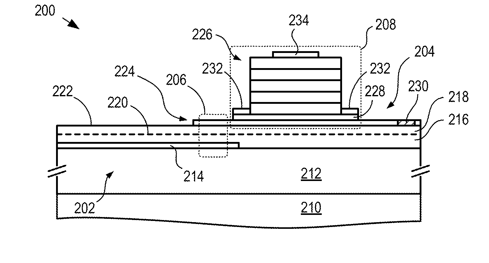
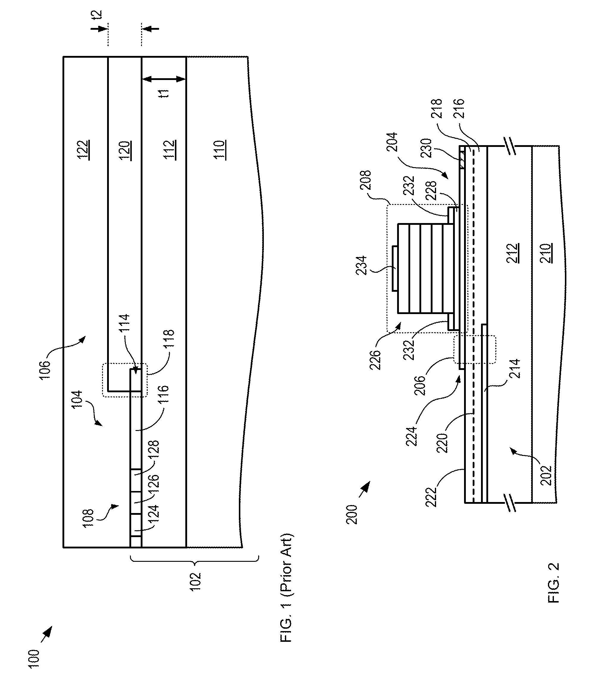
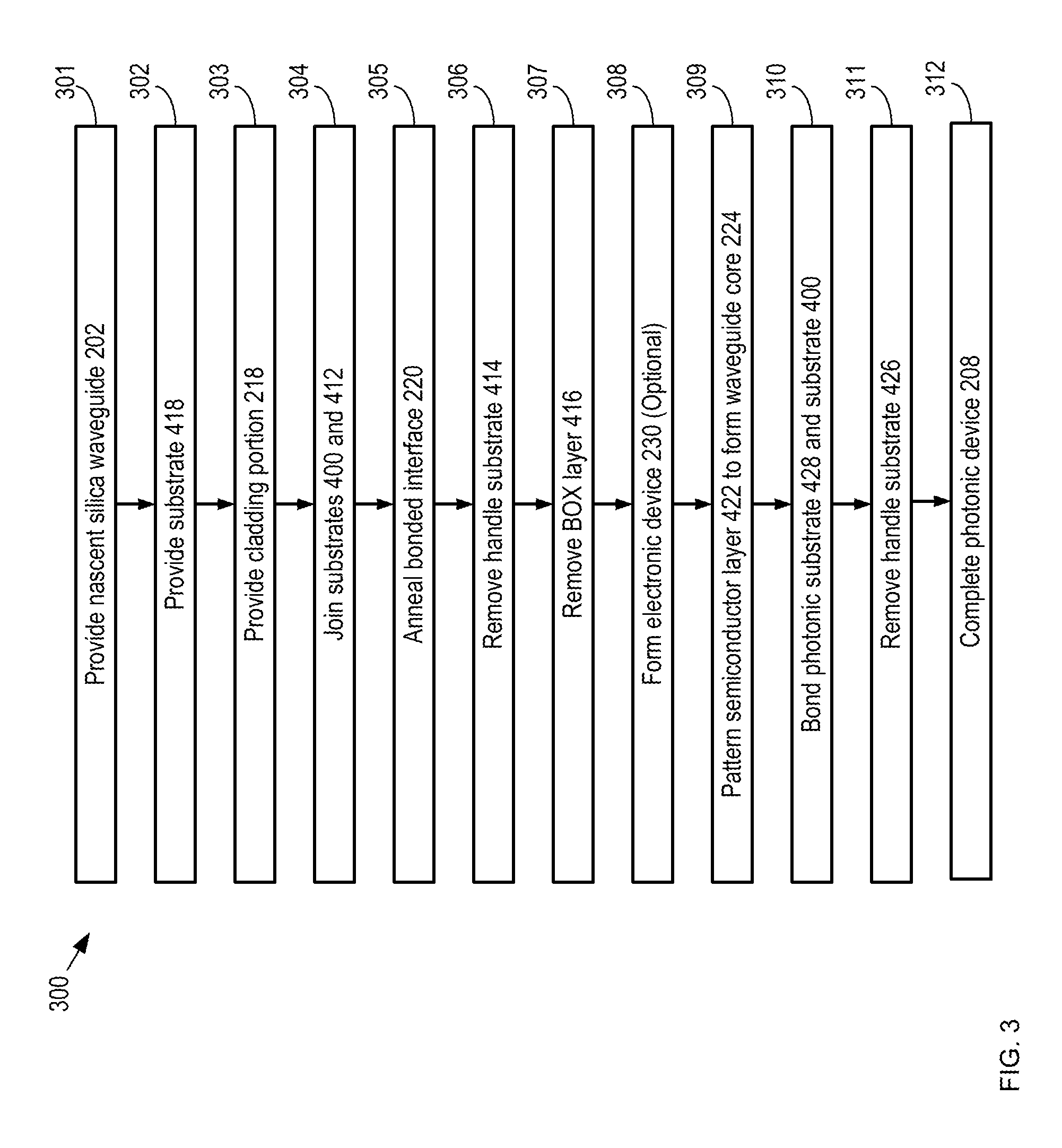
[0039]The following terms are defined for use in this Specification, including the appended claims:[0040]dielectric waveguide is defined as a waveguide comprising a waveguide core made of a material other than pure silicon. Examples of materials suitable for use in the waveguide core of a dielectric waveguide include, without limitation, silicon oxides (e.g., doped or undoped silicon dioxide, SiOx, etc.), silicon nitride, silicon oxynitride, silicon carbide, hafnium oxide, aluminum oxide, and silica.[0041]cladding layer is defined as a layer that is dimensioned and arranged to at least partially confine a propagating optical mode to a waveguide core. A cladding layer typically comprises a material that has a refractive index that is lower than that of the material of the waveguide core.[0042]heterogeneous silicon device is defined as a photonic device that includes a compound semiconductor layer structure that is heterogeneously integrated with a silicon layer or substrate by means ...


PUM


Abstract

A method for realizing a semiconductor waveguide and an ultra-low-loss dielectric waveguide disposed on the same substrate is disclosed. The method includes forming a partial dielectric waveguide structure on the substrate, wherein the dielectric waveguide is annealed to reduce hydrogen incorporation, and wherein the top cladding of the dielectric waveguide is only partially formed by a first dielectric layer. A second substrate comprising a semiconductor layer having a second dielectric layer disposed on its top surface is bonded to the first substrate such that the first and second dielectric layers collectively form the complete top cladding for the dielectric waveguide. The second substrate is then removed and the semiconductor layer is patterned to define the semiconductor waveguide core.

Description

STATEMENT REGARDING FEDERALLY SPONSORED RESEARCH[0001]This invention was made with Government support under Contract HR0011-09-C-0123 awarded by Defense Advanced Research Projects Agency (DARPA). The Government has certain rights in the invention.FIELD OF THE INVENTION[0002]The present invention relates to silicon-based photonics in general, and, more particularly, to the integration of low-loss, integrated-optic waveguides with a semiconductor layer suitable for forming semiconductor waveguides, active electronic devices, and active and passive photonic devices.BACKGROUND OF THE INVENTION[0003]Silicon-based photonics has grown to include dielectric waveguides, as well as silicon waveguides. A dielectric waveguide carries light in a central core made of an amorphous dielectric material, such as silicon nitride or silicon dioxide, and is typically formed on a silicon substrate. A silicon waveguide carries light in a core made of pure single-crystal silicon, which is typically formed ...

Claims


Application Information

Patent Timeline
Patent Type & Authority Patents(United States)
IPC IPC(8): G02B6/12H01L31/105G02B6/122G02B6/30G02B6/134G02B6/136
CPCG02B6/1225G02B6/1228G02B6/136G02B6/1347G02B6/305H01L31/105G02B2006/12176G02B2006/12188
Inventor BAUTERS, JAREDBOWERS, JOHN E.BOVINGTON, JOCKHECK, MARTIJNDAVENPORT, MICHAELBLUMENTHAL, DANIELBARTON, JONATHON SCOTT
Owner RGT UNIV OF CALIFORNIA
Why Eureka
Try Eureka