RF SOI switch with backside cavity and the method to form it

a soi switch and backside cavity technology, applied in the field of integrated circuits having transistors, can solve the problems of affecting performance and large capacitive coupling through the substrate, and achieve the effect of improving the performance of the integrated circuit and improving the radio frequency characteristics

Active Publication Date: 2016-03-22
SEMICON MFG INT (SHANGHAI) CORP
View PDF3 Cites 2 Cited by
  • Summary
  • Abstract
  • Description
  • Claims
  • Application Information

AI Technical Summary

Benefits of technology

[0007]In accordance with the invention, a circuit integrated (integrated circuit) into a substrate and having improved radio frequency characteristics includes a compound semiconductor substrate having a first semiconductor substrate, an insulating layer on the first semiconductor substrate, and a second semiconductor substrate on the insulating layer, and a transistor disposed in the second semiconductor substrate and having a bottom portion insulated by the insulating layer. The integrated circuit also includes a plurality of shallow trench isolations disposed on opposite sides of the transistor, a cavity disposed below (underneath) the bottom portion of the transistor, and a plurality of isolation plugs disposed on opposite sides of the cavity. By having a cavity located below the transistor, parasitic capacitive couplings between the source, drain of the transistor and the substrate are reduced and the performance of the integrated circuit is improved.

Problems solved by technology

However, due to the high frequency range in the radio frequency applications, source to drain leakage and parasitic capacitive coupling through the substrate can be relatively large and affect the performance (i.e., low insertion loss, good linear characteristics, and low signal distortion) of the field effect transistor.

Method used


Image

  • RF SOI switch with backside cavity and the method to form it
  • RF SOI switch with backside cavity and the method to form it
  • RF SOI switch with backside cavity and the method to form it

Examples


first embodiment

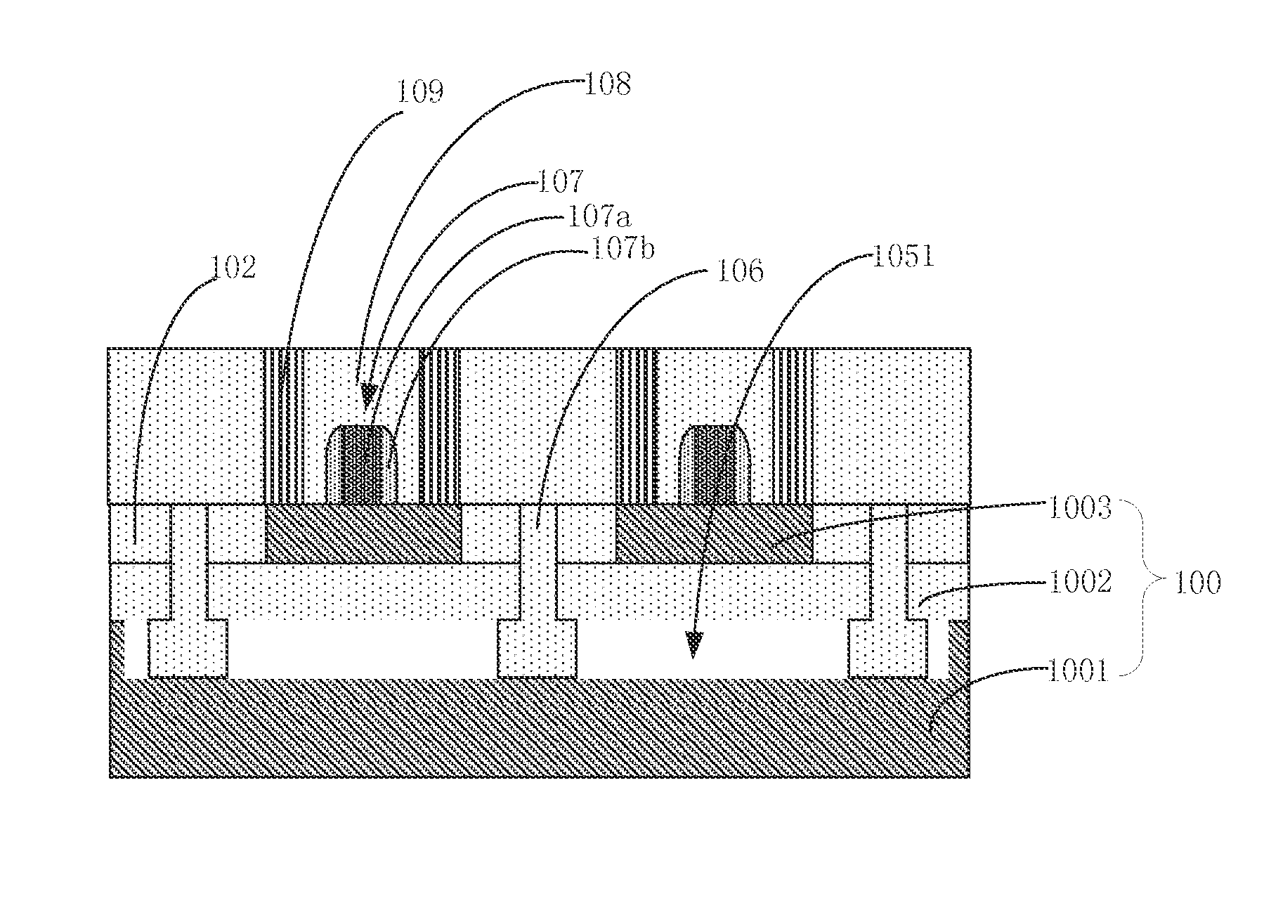
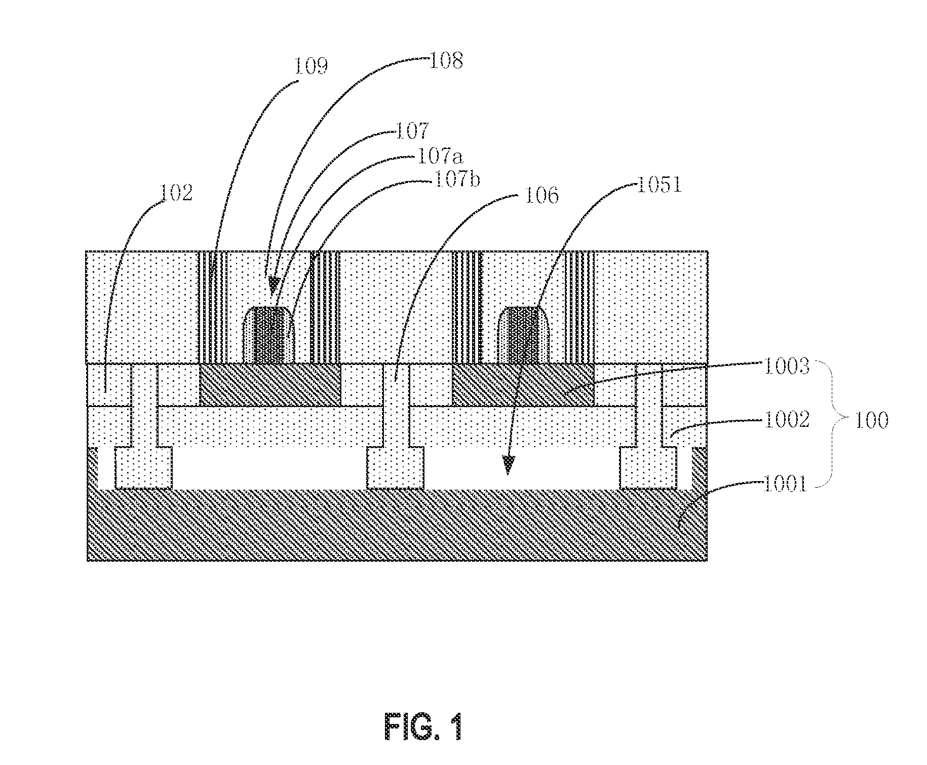
[0027]An integrated circuit includes a transistor disposed on a semiconductor substrate having a cavity disposed below (underneath) the transistor. The transistor can be isolated from the semiconductor substrate through the cavity, and the parasitic coupling between the source, the drain, and the gate of the transistor, and the parasitic capacitive coupling of the semiconductor substrate can be reduced to ultimately improve the performance of the integrated circuit.

[0028]FIG. 1 is a cross-sectional view of a structure of an integrated circuit according to an embodiment of the present invention. As shown in FIG. 1, the integrated circuit includes a compound semiconductor substrate 100 and a transistor 107 disposed in the compound semiconductor substrate. The compound semiconductor substrate includes a first semiconductor substrate 1001, an insulating layer 1002 on the first semiconductor substrate, and a second semiconductor substrate 1003 on the insulating layer. Transistor 107 is d...

second embodiment

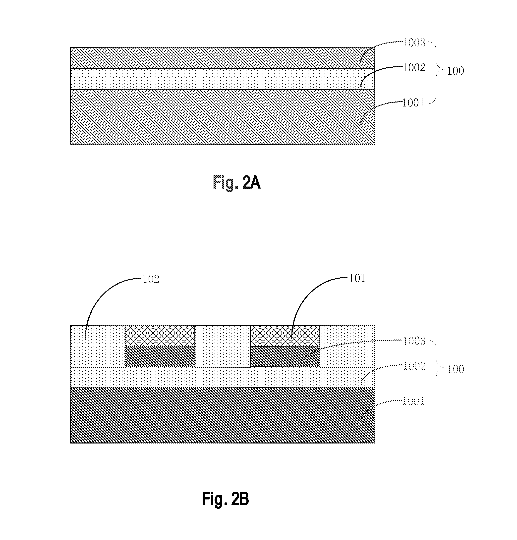
[0043]Referring to FIGS. 2A through 2F and FIG. 3, embodiments of the present invention provide a method of manufacturing an integrated circuit. FIGS. 2A through 2F are cross-sectional views of intermediate stages at different points during a manufacturing method of an integrated circuit, in accordance with an embodiment of the present invention.

[0044]According to an embodiment, a method of manufacturing an integrated circuit may include providing a compound semiconductor substrate having a first semiconductor substrate 1001, an insulating layer 1002 on first semiconductor substrate 1001, and a second semiconductor substrate 1002 on insulating layer 1002, as shown in FIG. 2A.

[0045]First semiconductor substrate 1001 is a silicon layer having a plane orientation (111), and second semiconductor substrate 1003 is a silicon layer having a plane orientation (111).

[0046]Insulating layer 1002 can be an oxide layer or a layer comprising any suitable insulating materials.

[0047]Because of the ...

third embodiment

[0074]Embodiments of the present invention also provide an electronic device. The electronic device includes the above-described integration circuit that is manufactured according to the method described above.

[0075]Because the integrated circuit has a cavity disposed below the transistor, coupling between the drain, source and gate of the transistor and between the semiconductor substrate can be significantly reduced to improve the performance of the electronic device. The integrated circuit according to embodiments of the present invention can be embedded in electronic devices that have a broad range of applications, such as, but not limited to, cellular phones, tablet PCs, netbooks, game consoles, portable DVD players, portable navigation systems, still and video cameras, digital voice recorders, MP3, MP4, and other electronic products.


PUM


Abstract

An integrated circuit includes a compound semiconductor substrate having a first semiconductor substrate, an insulating layer on the first semiconductor substrate, and a second semiconductor substrate on the insulating layer, a transistor disposed on the second semiconductor substrate and having a bottom insulated by the insulating layer, a plurality of shallow trench isolations disposed on opposite sides of the transistor, a cavity disposed below the bottom of the transistor, and a plurality of isolation plugs disposed on opposite sides of the cavity. By having a cavity located below the transistor, parasitic couplings between the transistor and the substrate are reduced and the performance of the integrated circuit is improved.

Description

CROSS-REFERENCES TO RELATED APPLICATIONS[0001]This application claims priority to Chinese patent application No. 201310627131.8, filed on Nov. 28, 2013, the content of which is incorporated herein by reference in its entirety.BACKGROUND OF THE INVENTION[0002]The present invention relates to semiconductor devices, and more particularly to an integrated circuit having a transistor for radio frequency applications and methods of manufacturing the same.[0003]A field effect transistor typically includes a silicon substrate, an impurity doped source and an impurity doped drain separated by a channel region. A gate insulation layer is disposed atop the channel region and a gate electrode made from electrically conductive material is located on top of the gate insulation layer.[0004]Field effect transistors are employed as switching devices in wireless communications devices, e.g., mobile phones, tablet PCs, and the like. A radio frequency (RF) switching device is typically a key component ...

Claims


Application Information

Patent Timeline
Patent Type & Authority Patents(United States)
IPC IPC(8): H01L27/12H01L21/762H01L21/84
CPCH01L27/1203H01L21/76232H01L21/76289H01L21/84H01L2924/0002H01L2924/00H01L23/552H01L23/66H01L29/045H01L29/0649H01L29/66651H01L29/7838H01L2223/6616
Inventor HUANG, HERB HEHONG, ZHONGSHAN
Owner SEMICON MFG INT (SHANGHAI) CORP
Why Eureka
Try Eureka