Flip-chip hybridisation of two microelectronic components using a UV anneal

a microelectronic component and anneal technology, applied in the field of flip-chip hybridization of two microelectronic components, can solve the problems of embrittlement of components, inability to withstand such temperatures, and disadvantages of submitting components to significant thermal shocks

Active Publication Date: 2016-04-19
COMMISSARIAT A LENERGIE ATOMIQUE ET AUX ENERGIES ALTERNATIVES
View PDF7 Cites 5 Cited by
  • Summary
  • Abstract
  • Description
  • Claims
  • Application Information

AI Technical Summary

Benefits of technology

[0005]The present invention aims at providing a method of manufacturing a device comprising a first and a second components hybridized by means of electric interconnects, which does not require taking the entire device to a high temperature to form said interconnects.
[0017]In other words, it is possible to control the copper oxide portion which is reduced into copper by delimiting it with a region which absorbs or reflects ultraviolet radiation. It is thus possible to form interconnects accurately limited in space, even in the case where a copper oxide ink, which spreads once deposited, is used.
[0018]According to an embodiment, the second component is made of PEN, PET, or glass, which materials are transparent to UVs and inexpensive. Further, PEN and PET have the advantage of being flexible materials.

Problems solved by technology

This type of hybridization however has the disadvantage of submitting the components to a significant thermal shock, the melting temperature of the materials of the bumps being usually greater than 152° C., this temperature being the melting temperature of the solder material, that is, tin.
Such a heating may thus embrittle the components and / or forbid the use of materials which cannot withstand such temperatures, such as plastic materials, particularly PEN (polyethylene naphthalate) and PET (polyethylene terephthalate), which have a vitreous transition temperature usually much lower than the melting temperature of the solder materials.

Method used


Image

  • Flip-chip hybridisation of two microelectronic components using a UV anneal
  • Flip-chip hybridisation of two microelectronic components using a UV anneal
  • Flip-chip hybridisation of two microelectronic components using a UV anneal

Examples


Embodiment Construction

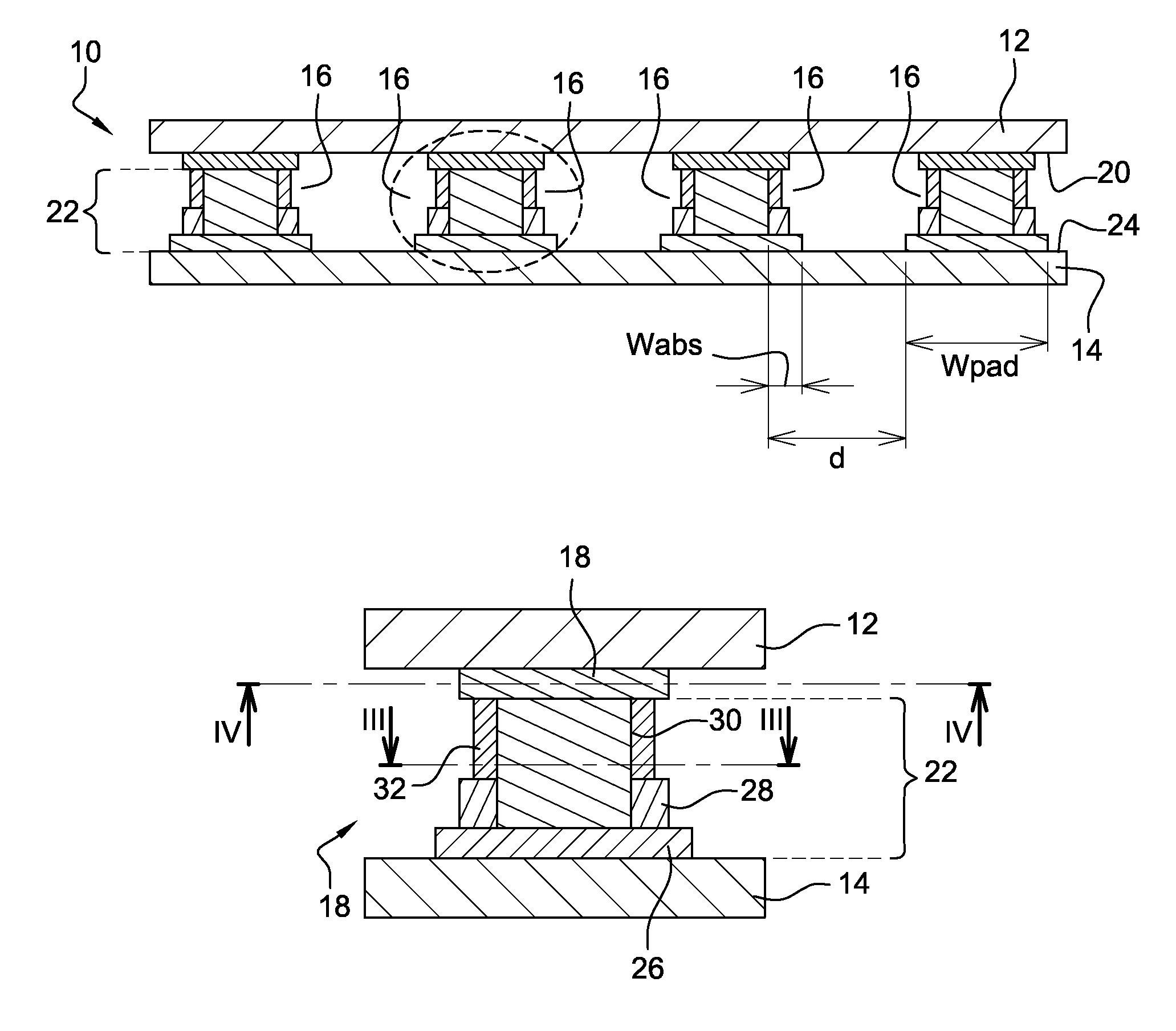
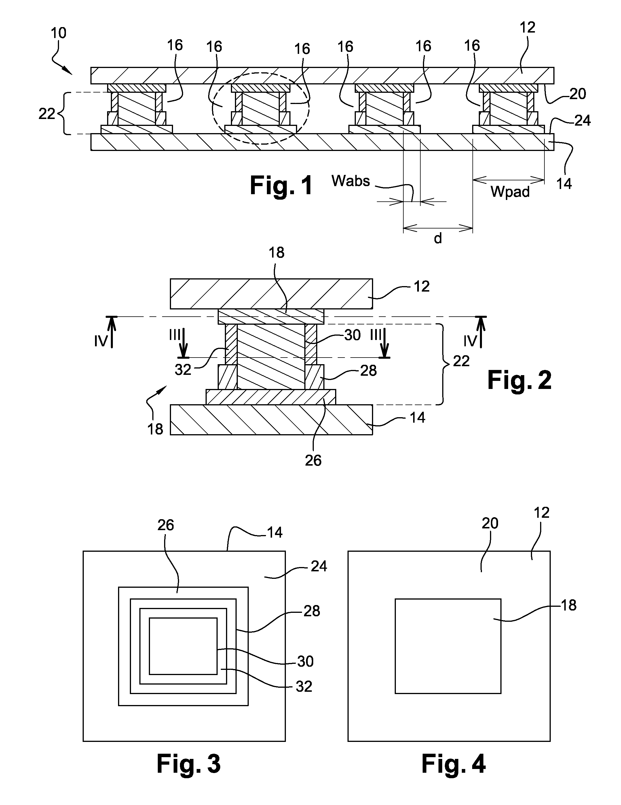
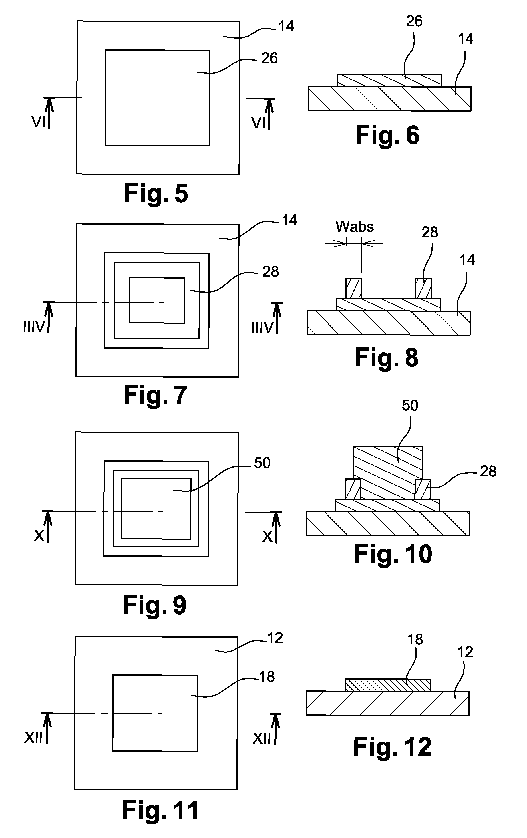
[0031]A device 10 according to the invention will be described in relation with FIGS. 1 to 4. Device 10 comprises a first and a second components 12, 14 hybridized to each other by mean of electric interconnects 16. First component 12 for example comprises an array of photosensitive elements, and the second component for example comprises a circuit for reading said array, interconnects 16 connecting each photosensitive element of the array to the read circuit. The second component is further transparent to ultraviolet radiation at least in line with interconnects 16. Particularly, the second component may be essentially made of flexible, low-cost and transparent plastic materials, such as PEN or PET, or also be made of glass, in which case the second component is transparent over its entire surface.

[0032]Interconnects 16 each comprise a solid conductive area 18 formed on a surface 20 of first component 12, for example, a metal area made of gold, silver, copper, platinum, titanium, o...


PUM


Abstract

A method of manufacturing a microelectronic device including a first component hybridized with a second component via electric interconnects, involves the steps of: (i) forming the first and second components, the second component being transparent to ultraviolet radiation at least in line with locations provided for the interconnects; (ii) forming interconnection elements including copper oxide on the second component at the locations provided for the interconnects; (iii) placing the first and second components on each other; and (iv) applying the ultraviolet radiation through the second component on the elements including copper oxide to implement an ultraviolet anneal converting copper oxide into copper.

Description

FIELD OF THE INVENTION[0001]The invention relates to the “flip-chip” hybridization of two microelectronic components.BACKGROUND OF THE INVENTION[0002]Flip-chip hybridization is a technique where two microelectronic components, for example, an array of photosensitive elements and a circuit for reading it, are independently formed, and where these components are placed on each other while electric interconnects, necessary to their operation, are formed therebetween.[0003]According to the state of the art, the interconnects are made in the form of solder bumps, arranged between metal areas wettable by the material forming the bumps, formed on opposite surfaces of the components. The hybridization method then comprises forming said areas on the surfaces of the components to be hybridized, depositing a solder material on the areas of a first component, placing the second component on the first component while aligning the areas of the two components, and then heating the assembly to a te...

Claims


Application Information

Patent Timeline
Patent Type & Authority Patents(United States)
IPC IPC(8): H01L21/00H01L21/48H01L23/498H01L23/14H01L23/00H01L21/56
CPCH01L24/03H01L21/4867H01L23/145H01L23/49811H01L24/05H01L24/11H01L24/13H01L24/16H01L24/81H01L2224/81192H01L2224/81409H01L2224/81948H01L2224/83102H01L2924/00014H01L21/563H01L2224/0219H01L2224/02166H01L2224/02175H01L2224/0345H01L2224/0361H01L2224/03848H01L2224/0401H01L2224/05541H01L2224/05568H01L2224/05573H01L2224/05639H01L2224/05644H01L2224/05647H01L2224/05666H01L2224/05669H01L2224/10156H01L2224/10175H01L2224/1131H01L2224/11332H01L2224/11515H01L2224/11848H01L2224/13007H01L2224/13109H01L2224/13111H01L2224/13147H01L2224/13187H01L2224/1601H01L2224/16505H01L2224/29035H01L2224/73103H01L2224/73203H01L2224/818H01L2224/819H01L2224/8123H01L2224/8184H01L2224/81121H01L2224/81224H01L2924/01029H01L2924/053H01L2924/0105H01L2924/01079H01L2924/01047H01L2924/01022H01L2924/20754H01L2924/00012H01L2224/05552
Inventor ALIANE, ABDELKADERCOPPARD, ROMAINTALLAL, JAMAL
Owner COMMISSARIAT A LENERGIE ATOMIQUE ET AUX ENERGIES ALTERNATIVES
Why Eureka
Try Eureka