Electro-optical transceiver device to enable chip-to-chip interconnection

a technology of optical communication and transceiver, which is applied in the direction of optical elements, instruments, optical radiation measurement, etc., can solve the problems of reducing reducing the speed of communication, and reducing the performance of the device, so as to reduce the size of the device, reduce the number of assembly operations, and reduce the cost of manufacturing and assembly.

Active Publication Date: 2016-04-26
QUALCOMM INC
View PDF8 Cites 2 Cited by
  • Summary
  • Abstract
  • Description
  • Claims
  • Application Information

AI Technical Summary

Benefits of technology

[0004]A device may include a substrate, such as a glass interposer. The substrate may be coupled to a printed circuit board (PCB) and further coupled to an optical channel (e.g., a waveguide) that communicates information between components (e.g., a processor and / or a memory) of the device. The substrate may have a configuration that integrates electro-optical functionalities and components. For example, the substrate may include one or more lens arrays, traces, waveguides, and / or electrical interconnects (i.e., one or more lens arrays, traces, waveguides, electrical interconnects, and / or other components may be integrated within the substrate). A waveguide may be coupled to a surface of the substrate. Alternatively or in addition, the substrate may include a waveguide (i.e., the waveguide may be integrated within the substrate). The substrate may enable reduced fabrication and assembly costs as compared to conventional electro-optical assembly processes (e.g., by reducing a number of assembly operations relative to conventional electro-optical assembly processes). For example, the substrate may enable a device manufacturer to avoid complex assembly of separate components such as silicon (Si) carriers, organic cutout substrates, and / or lens arrays. Further, by integrating components within the substrate, a size (or “form factor”) of a device may be reduced as compared to a device assembled using a conventional assembly process.
[0009]A particular advantage provided by at least one of the disclosed embodiments is that an electro-optical transceiver device that includes optical components on a substrate can be manufactured using fewer process operations. As an example, a waveguide of the electro-optical transceiver device and components of the electro-optical transceiver device may be coupled to the same substrate. Alternatively or in addition, the substrate may include a waveguide, which may reduce assembly costs associated with connecting devices to the waveguide. Further, a size (or “stack height”) of the device can be reduced as compared to an electro-optical transceiver device that utilizes discrete components and metal interconnections (instead of a glass interposer). An electro-optical transceiver device in accordance with the present disclosure may enable higher bus throughput, fewer interconnect pins, less crowded logic to logic routing, and / or longer interconnects without deterioration in signal quality. Other aspects, advantages, and features of the present disclosure will become apparent after review of the entire application, including the following sections: Brief Description of the Drawings, Detailed Description, and the Claims.

Problems solved by technology

Assembling semiconductor devices on a circuit board to enable optical communication may be expensive and complicated.
These electronic devices may have reduced performance (e.g., lower speed communications) as compared to electronic devices that include optically-coupled semiconductor chips.

Method used


Image

  • Electro-optical transceiver device to enable chip-to-chip interconnection
  • Electro-optical transceiver device to enable chip-to-chip interconnection
  • Electro-optical transceiver device to enable chip-to-chip interconnection

Examples


Embodiment Construction

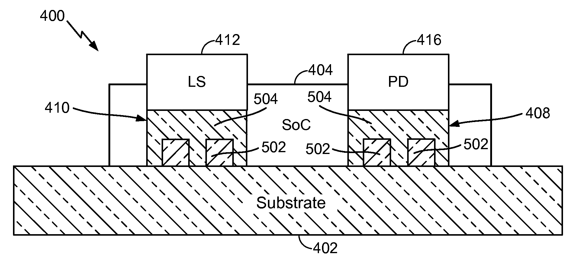
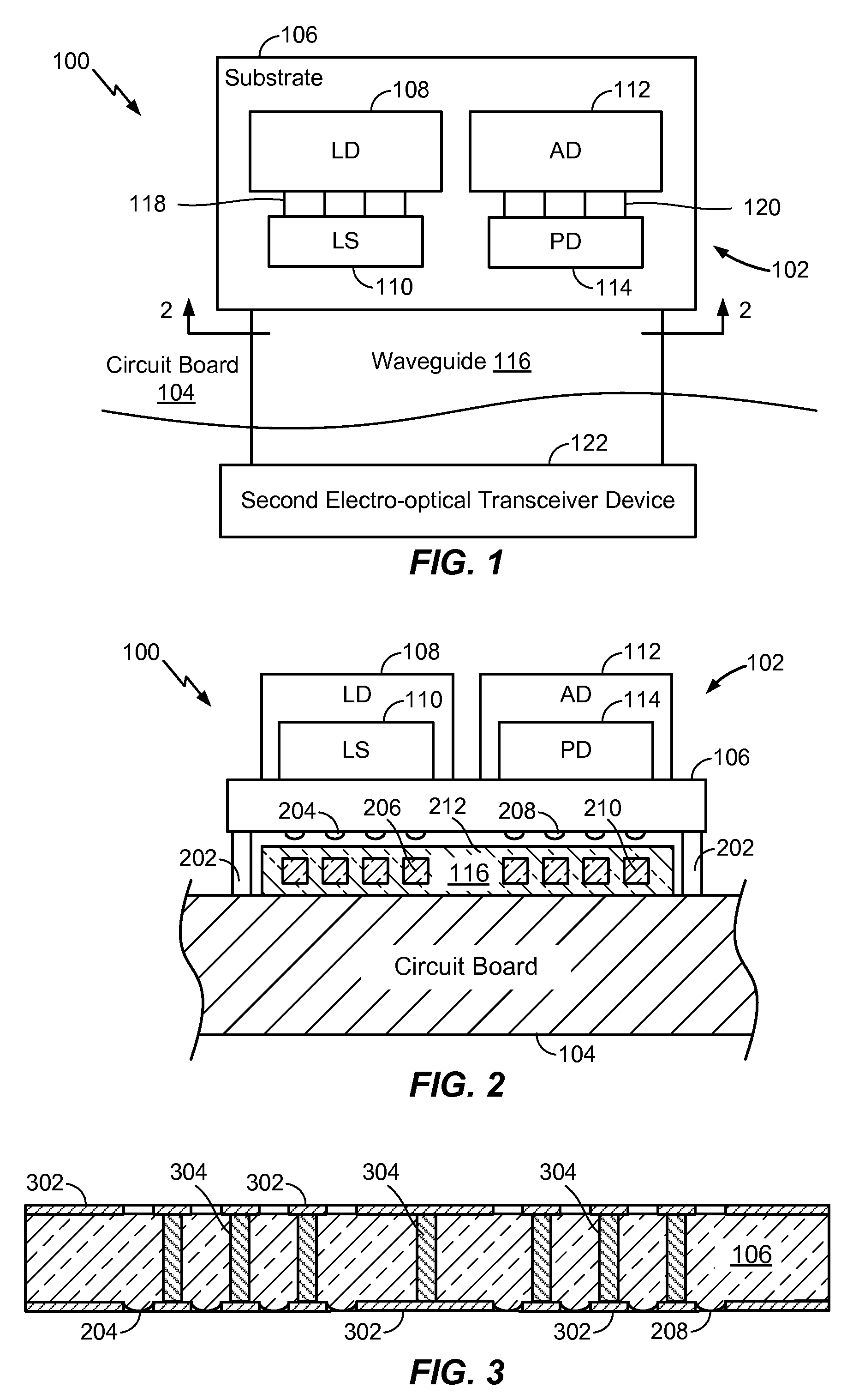
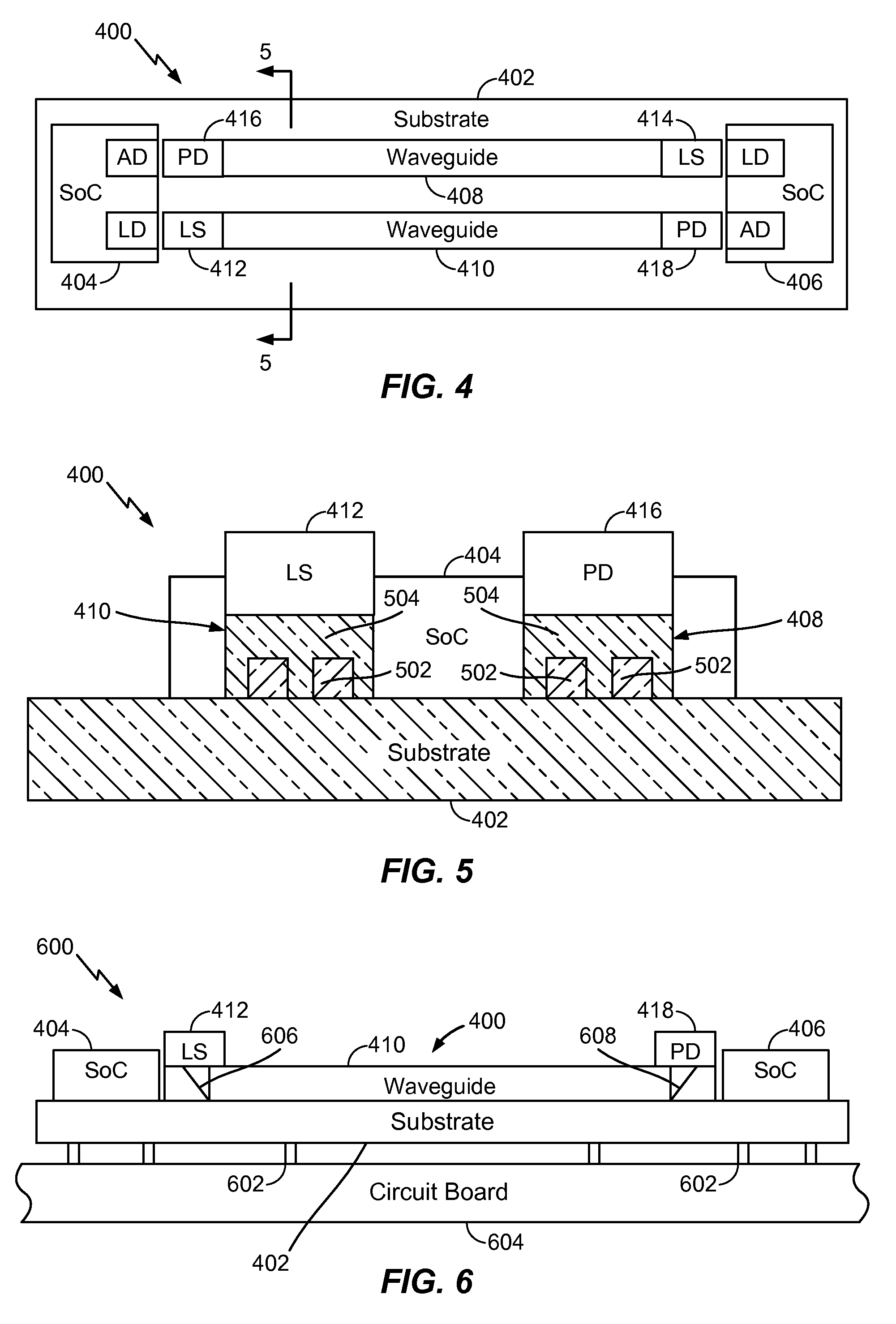
[0022]Particular embodiments of devices that include an electro-optical transceiver device to enable chip-to-chip communication are presented in this disclosure. The chip-to-chip communication may be between chips coupled to a single circuit board or between a chip mounted on a first circuit board and a second chip mounted on a second circuit board. It should be appreciated, however, that the information described for particular embodiments with respect to the designs of devices may be embodied in a variety of contexts. The particular embodiments presented are merely illustrative and do not limit the scope of this disclosure.

[0023]The present disclosure describes particular embodiments in specific contexts. However, features, methods, structures or characteristics described according to the particular embodiments may also be combined in suitable manners to form one or more other embodiments. In addition, figures are used to illustrate the relative relationships between the features,...


PUM


Abstract

An apparatus includes a substrate and a waveguide coupled to a surface of the substrate. The surface forms a cladding layer of the waveguide. The apparatus includes a photodetector optically coupled to an end of the waveguide. The photodetector is configured to output an electrical signal responsive to receiving a light signal from a core of the waveguide. The apparatus also includes an amplifier device coupled to the substrate. The amplifier device is electrically coupled to the photodetector to amplify the electrical signal to produce an amplified electrical signal.

Description

FIELD[0001]The present disclosure is generally related to an electro-optical transceiver device to enable chip-to-chip interconnection.DESCRIPTION OF RELATED ART[0002]An electronic device may include semiconductor devices (or semiconductor “chips”) attached to a circuit board. For example, a mobile electronic device may include a processor and a memory attached to a circuit board. The semiconductor devices may communicate using connections, such as metal interconnects. To increase communication speed and / or quality, the semiconductor devices may be connected using optical (or electro-optical) interconnections. To illustrate, a semiconductor device may send data to and receive data from another semiconductor device by modulating data onto an optical signal and by transmitting the optical signal via an optical communication channel.[0003]Assembling semiconductor devices on a circuit board to enable optical communication may be expensive and complicated. For example, a process to assem...

Claims


Application Information

Patent Timeline
Patent Type & Authority Patents(United States)
IPC IPC(8): H04B10/00G02B6/00G01J1/04H03F3/08G02B6/42G02B6/43H04B10/50
CPCH04B10/50G01J1/0407G02B6/00G02B6/428G02B6/4212G02B6/43H03F3/08H04B10/501G02B6/4204G02B6/4274H04B10/60
Inventor LAI, KWAN-YUSHENOY, RAVINDRA VAMANKIM, JITAELASITER, JON BRADLEYKIDWELL, JR., DONALD WILLIAMGOUSEV, EVGENI PETROVICH
Owner QUALCOMM INC
Why Eureka
Try Eureka