Method for chemical mechanical polishing of high-K metal gate structures

a metal gate structure and high-k technology, applied in the direction of semiconductor devices, electrical equipment, transistors, etc., can solve the problems of serious polysilicon gate over-polishing, etc., to achieve the effect of easy removal of a hard mask layer without affecting the performance and yield of the manufactured semiconductor devi

Active Publication Date: 2016-05-10
SEMICON MFG INT (SHANGHAI) CORP
View PDF1 Cites 2 Cited by
  • Summary
  • Abstract
  • Description
  • Claims
  • Application Information

AI Technical Summary

Benefits of technology

[0010]Embodiments of the present invention provide a method for manufacturing a semiconductor device structure and a semiconductor device that can easily remove a hard mask layer without impacting the performance and yield of the semiconductor device.
[0011]In accordance with the present invention, a method for manufacturing a semiconductor device includes providing a substrate, a dielectric layer on the substrate, a first hard mask layer on the substrate, and a second hard mask layer on the first hard mask layer. The method also includes removing the first hard mask layer using a reactive gas that is not susceptible to cause damage to the dielectric layer to improve the performance and yield of the semiconductor device.

Problems solved by technology

Since a conventional CMP process utilizes a polish slurry that has a polysilicon removal rate greater than the aluminum removal rate, polysilicon gates tend to be over-polished.
Furthermore, an over-polishing of polysilicon gates may occur during the CMP process of the aluminum gates of the N-type transistors.
As can be clearly seen, the height of the polysilicon gate transistor region is significantly reduced due to over-polishing, which seriously affects the performance and yield of the manufactured semiconductor device.
This can adversely affect the performance and yield of the semiconductor device.
The over-etching causes undue etching of the interlayer dielectric layer, which is located below the portion of the hard mask to be removed, leading to a loss of the thickness of the interlayer dielectric layer.
The thickness loss of the interlayer dielectric layer, in turn, causes a loss of thickness of the polysilicon gate of the polysilicon gate transistor region, which negatively impacts the performance and yield of the semiconductor device.

Method used


Image

  • Method for chemical mechanical polishing of high-K metal gate structures
  • Method for chemical mechanical polishing of high-K metal gate structures
  • Method for chemical mechanical polishing of high-K metal gate structures

Examples


embodiment 1

[0039]FIGS. 2A to 2F are cross-sectional views depicting stages of a method of manufacturing a semiconductor device according to an embodiment of the present invention, and FIG. 3 is a simplified flow chart of a method of manufacturing a semiconductor device according to an embodiment of the present invention. With reference to FIGS. 2A-2F and FIG. 3, a method according to the embodiment includes the following steps:

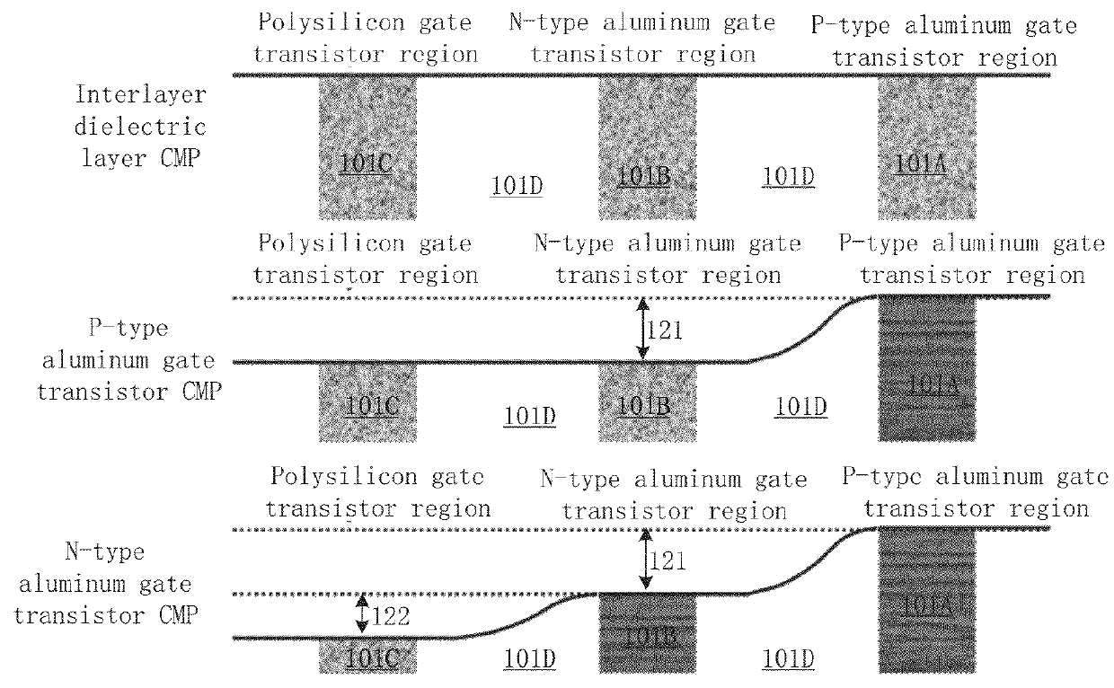
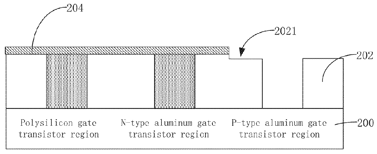
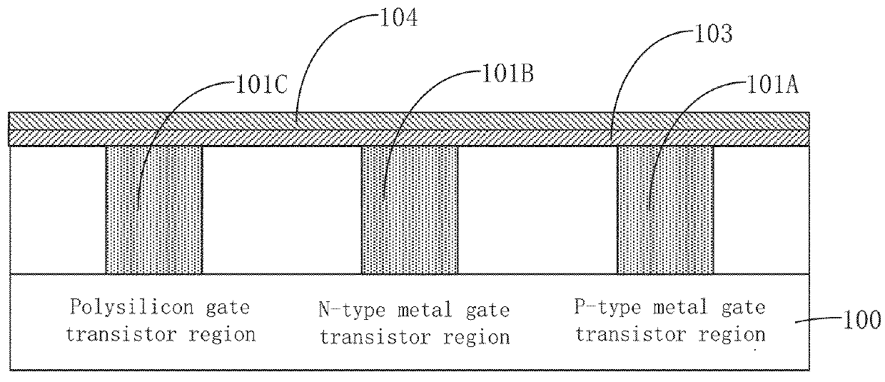
[0040]Step A1: provide a semiconductor substrate 100 comprising a front-end device, the front-end device comprises a P-type metal gate transistor region having a first dummy gate 101A, an N-type metal gate transistor region having a second dummy gate 101B, and a polysilicon gate region having a polysilicon gate 101C; form an interlayer dielectric layer on the semiconductor substrate, as shown in FIG. 2A.

[0041]In the embodiment, the front-end device is referred to as a structure that has been formed on the semiconductor substrate and may contain certain components, but th...

embodiment 2

[0069]FIG. 3 is a simplified flow chart of a method 300 for manufacturing a semiconductor device according to an embodiment of the present invention. Method 300 includes:

[0070]S101: provide a semiconductor substrate comprising a front-end device, the front-end device comprises a first type metal gate transistor region, a second type metal gate transistor region, and a polysilicon gate transistor region, the first type metal gate transistor region comprises a first dummy gate, the second type metal gate transistor region comprises a second dummy gate, the polysilicon gate transistor region comprises a polysilicon gate; form an interlayer dielectric layer on the semiconductor substrate;

[0071]S102: form a first hard mask layer on the interlayer dielectric layer; form a second hard mask layer on the first hard mask layer;

[0072]S103: form a mask layer on the second hard mask layer, the mask layer having an opening for exposing a portion of the second hard mask layer located above the fir...


PUM

PropertyMeasurementUnit
work functionaaaaaaaaaa
pressureaaaaaaaaaa
gas flow rateaaaaaaaaaa

Abstract

A method for manufacturing a semiconductor device includes providing a substrate, a dielectric layer on the substrate, a first hard mask layer on the substrate, and a second hard mask layer on the first hard mask layer. The method also includes removing the first hard mask layer using a reactive gas that does not cause damage to the dielectric layer to improve the performance and yield of the semiconductor device.

Description

CROSS-REFERENCES TO RELATED APPLICATIONS[0001]This application claims priority to Chinese patent application No. 2014101226194.7, filed on May 26, 2014, the content of which is incorporated herein by reference in its entirety.BACKGROUND OF THE INVENTION[0002]The present invention relates to semiconductor devices and the fabrication of semiconductor devices, and more particularly to semiconductor devices in 32 nm technology nodes and beyond.[0003]In the field of semiconductor technology, aluminum or aluminum alloy is mainly used in high-k metal gate (HKMG) process technology nodes at 32 nm and below (e.g., 28 nm). The use of aluminum or aluminum alloy for metal gate electrodes has cost and performance advantages. The aluminum gate chemical mechanical polishing (CMP) process is a very important process for manufacturing high-k metal gate transistors having aluminum gates.[0004]In order to increase the gap filling space, a CMP process of aluminum gates typically includes two steps: a C...

Claims


Application Information

Patent Timeline
Patent Type & Authority Patents(United States)
IPC IPC(8): H01L21/8234H01L21/28H01L27/088
CPCH01L21/82345H01L21/28008H01L27/088H01L29/66545H01L21/823842
Inventor NI, JINGHUAZHAO, JIANWU, LEI
Owner SEMICON MFG INT (SHANGHAI) CORP
Why Eureka
Try Eureka