CMOS input buffer circuit
a technology of input buffer and cmos, which is applied in the direction of logic circuit coupling/interface arrangement, power consumption reduction, pulse technique, etc., can solve the problem that the linearity improvement technology of bjt input buffer does not work for cmos type, the layout size is larger, and the power consumption is much more holistic, so as to facilitate its realization, wide application range, and low cost
- Summary
- Abstract
- Description
- Claims
- Application Information
AI Technical Summary
Benefits of technology
Problems solved by technology
Method used
Image

Examples
embodiment 1
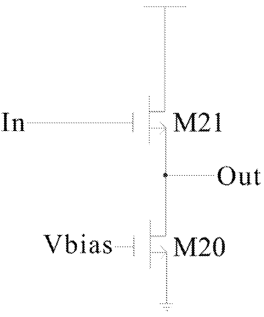
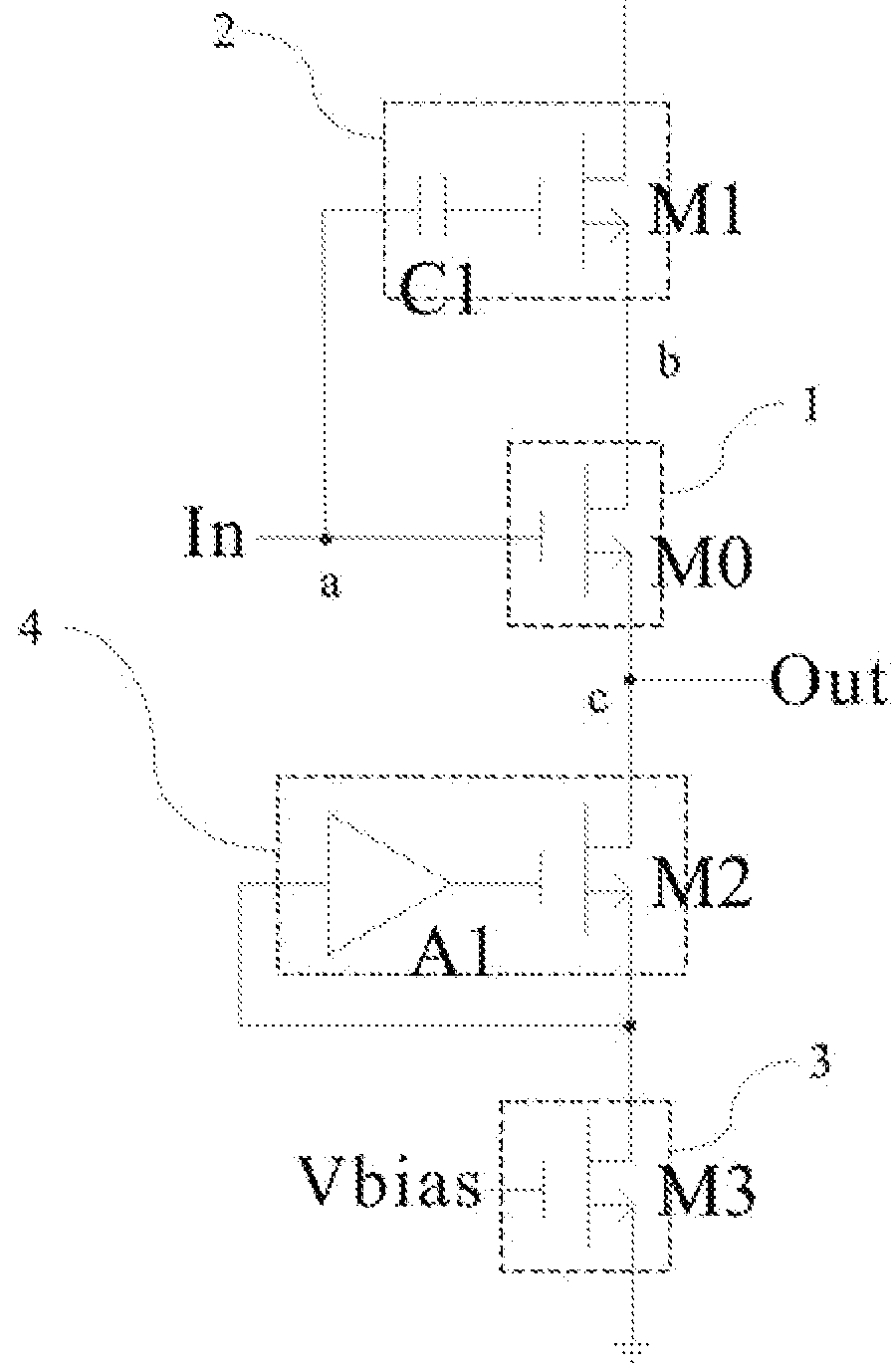
[0031]As shown in FIG. 2, a CMOS input buffer circuit includes a CMOS input follower circuit, a linearity improvement circuit of follower transistor, a current source load, and a linearity improvement circuit of load impedance.
[0032]The CMOS input follower circuit follows changes of input signals and outputs follower input signals. The CMOS input follower circuit includes a M0 NMOS (N-Channel MOS) transistor. A gate of the M0 NMOS serves as an input end of the CMOS input follower circuit. A source of the M0 NMOS serves as an output end of the CMOS input follower circuit. The linearity improvement circuit of follower transistor is connected between the gate and the drain of the M0 NMOS transistor. An end of the linearity improvement circuit of load impedance is connected to the source of the M0 NMOS transistor. The other end of the linearity improvement circuit of load impedance is connected to the current source load.
[0033]The linearity improvement circuit of follower transistor (M0...
embodiment 2
[0048]The difference between embodiment 2 and embodiment 1 is related as follows.
[0049]FIG. 3 is preferred embodiment 2 of high linearity CMOS input buffer.
[0050]FIG. 3 shows that M0, M1, M2 and M3 transistors are PMOS transistors in embodiment 2. As load transistor is PMOS type, impedance slightly drops. Yet, the substrate of PMOS transistor can be connected to level in ways that provide a higher linearity of input follower transistor than that in embodiment 1.
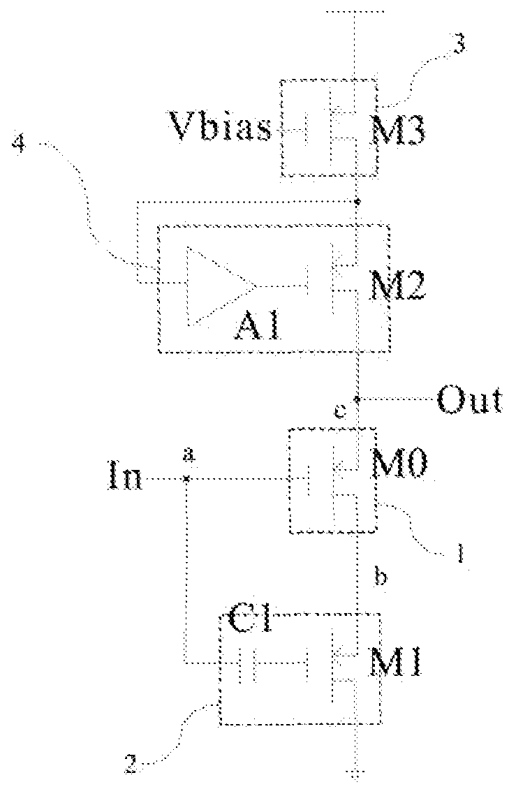
embodiment 3
[0051]The difference between embodiment 3 and embodiment 1 is related as follows.
[0052]FIG. 4 is preferred embodiment 3 of high linearity CMOS input buffer.
[0053]FIG. 4 shows that operational amplifier A1 is taken out and M4 NMOS transistor is added to the circuit. The drain of M4 NMOS transistor is connected to the source of M2 NMOS transistor and the source of M4 NMOS transistor is connected to the drain of M3 NMOS transistor. The gates of M2 NMOS transistor and M4 NMOS transistor are connected to bias voltage. In doing so, power consumption drops. The M4 MOS transistor restrains output swing.
PUM
 Abstract
Description
Claims
Application Information
 - R&D
- Intellectual Property
- Life Sciences
- Materials
- Tech Scout
- Unparalleled Data Quality
- Higher Quality Content
- 60% Fewer Hallucinations
Browse by: Latest US Patents, China's latest patents, Technical Efficacy Thesaurus, Application Domain, Technology Topic, Popular Technical Reports.
© 2025 PatSnap. All rights reserved.Legal|Privacy policy|Modern Slavery Act Transparency Statement|Sitemap|About US| Contact US: help@patsnap.com