Method of forming source/drain contacts in unmerged FinFETs

Active Publication Date: 2016-06-28
ELPIS TECH INC
View PDF8 Cites 17 Cited by
  • Summary
  • Abstract
  • Description
  • Claims
  • Application Information

AI Technical Summary

Benefits of technology

This patent text describes how the invention can improve the performance and minimize the contact resistance of FinFET Integrated Circuit (IC) chips, which can lead to better overall performance.

Problems solved by technology

The narrow parallel fins form non-planar source and drain regions make it challenging to contact FinFET source / drains.
Unfortunately, the RIE is non-selective and etches off the highly conductive epi at source / drain regions, reducing the area available for contacts.
Consequently, the loss of available contact area results in higher resistance (Rs) in subsequently formed contacts.
Rs is a series resistance that adds to device on impedance, and as such, reduces drive current, which reduces circuit performance.
Previous approaches to minimizing the reduction in contact area have added fabrication steps, e.g., covering gates with nitride, that increased fabrication complexity and resulting fabrication costs.

Method used


Image

  • Method of forming source/drain contacts in unmerged FinFETs
  • Method of forming source/drain contacts in unmerged FinFETs
  • Method of forming source/drain contacts in unmerged FinFETs

Examples


Embodiment Construction

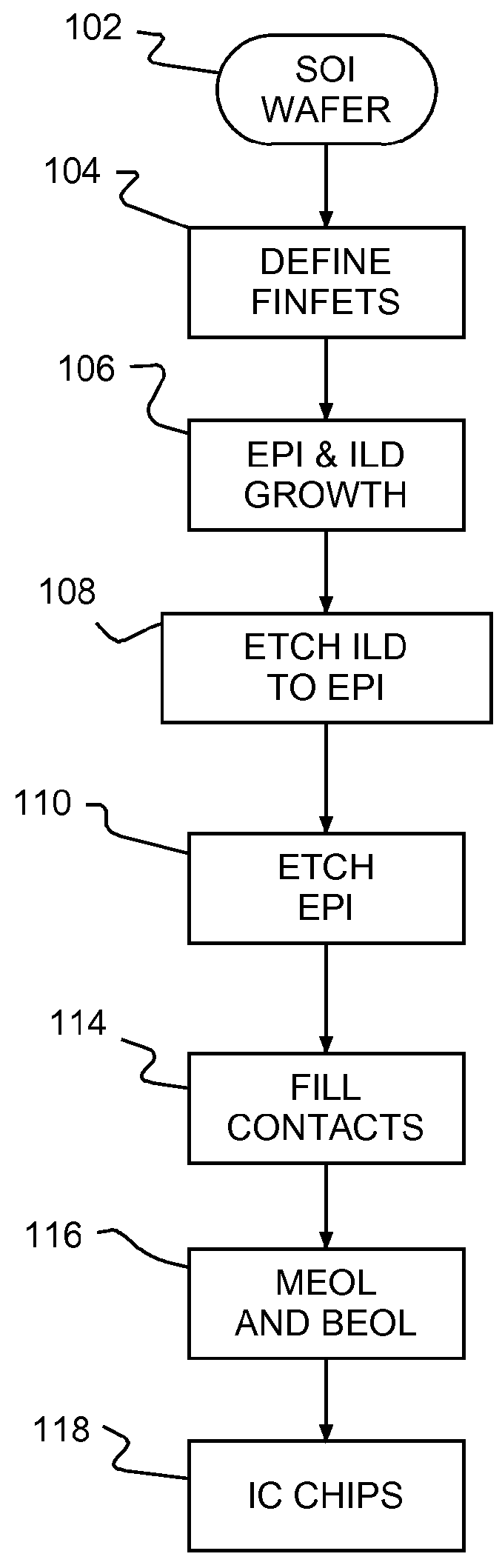
[0022]Turning now to the drawings and, more particularly, FIG. 1 shows an example of a preferred method of forming field effect transistors (FETs), e.g., in an integrated circuit (IC), and more particularly, forming unmerged epitaxially-grown semiconductor (epi) FinFETs according to a preferred embodiment of the present invention. Preferred unmerged FinFETs are covered by a contact dielectric or inter-level dielectric (ILD) layer. A timed etch of the ILD exposes the tops of the unmerged epi for contact formation. Etching through the epi into buried fins leaves the highly doped source / drain epi intact and increases contact area, reducing contact resistance over contacts formed using prior contact formation methods.

[0023]Fabrication begins in step 102 with providing a typical semiconductor wafer, e.g., a bulk semiconductor wafer, or as shown in this example, a silicon on insulator (SOI) wafer. In step 104 chip devices (FETs) are defined, e.g., by defining and forming fins in a surface...


PUM


Abstract

A method of forming field effect transistors (FETs), and forming integrated circuit (IC) chip including the FETs. After forming replacement metal gate (RMG) FinFETs on a surface layer of a silicon on insulator (SOI) wafer, and growing unmerged epitaxially (epi) on the fins, the epi is capped with dielectric and an inter-level dielectric (ILD) layer is formed on the SOI wafer. The said ILD layer is patterned to an upper surface of the epi above encased fins in a timed etch. Then, etching, preferably with an etchant selective to silicon, the epi is opened to, and into, the fins. The resulting orifices are filled with conductive material to form source drain contacts.

Description

BACKGROUND OF THE INVENTION[0001]1. Field of the Invention[0002]The present invention is related to semiconductor devices and manufacturing, and more particularly, to forming fin field effect transistors (FinFETs) on semiconductor wafers and methods of manufacturing Integrated Circuits (ICs) with circuits including multi-fin FinFETs.[0003]2. Background Description[0004]Integrated Circuit (IC) chip density and performance are primary semiconductor technology development goals. Semiconductor technology and chip manufacturing advances have improved performance through a steady increase of on-chip clock frequencies, coupled with a corresponding decrease in chip supply voltage resulting in part from reduced chip feature size.[0005]To minimize power consumption, typical ICs are made in the well-known complementary insulated gate field effect transistor (FET) technology known as CMOS. A typical CMOS circuit includes paired complementary devices, i.e., an n-type FET (NFET) paired with a cor...

Claims


Application Information

Patent Timeline
IPC IPC(8): H01L29/78H01L21/8238H01L21/8234H01L21/02H01L21/311H01L21/283H01L27/092
CPCH01L21/823821H01L21/823418H01L21/02304H01L21/31144H01L21/283H01L27/0924H01L21/76805H01L21/76897
Inventor BASKER, VEERARAGHAVANCHENG, KANGGUOKHAKIFIROOZ, ALI
Owner ELPIS TECH INC
Why Eureka
Try Eureka