Crystalline surface structures and methods for their fabrication

a crystalline surface and structure technology, applied in the field of film growth technology, can solve the problems of limiting the commercial lifetime of fcs-structures, reducing or negating many useful properties, and time-consuming and expensive manufacturing of fcs-structures in general and devices based on individual fcs-structures, so as to achieve simple, cheaper and more versatile methods, and improve performance. the effect of performan

Inactive Publication Date: 2016-07-19
CANATU OY
View PDF8 Cites 2 Cited by
  • Summary
  • Abstract
  • Description
  • Claims
  • Application Information

AI Technical Summary

Benefits of technology

[0032]A further advantage of the present invention is that it provides a method for fabricating crystalline structures, specifically FCS-structures, on a template from which the FCS-structures can be easily transferred onto secondary, e.g. polymer, substrates or integrated into electronic devices. By impregnating the template with different elements the resulting FCS-structures can be fabricated in different compositions comprising these different elements. The method according to the present invention allows for simpler, cheaper and more versatile method for fabricating FCS-structures than prior art techniques, thus allowing reduced cost and better performance.
[0033]The invention is particularly useful in, for example, the manufacturing of homogeneous or patterned transparent, conductive, and flexible polymer films comprising graphene or other FCS-structures. The invention may also be used in the fabrication of e.g. coated and multi-layered or three-dimensional structures, which are suitable for many optical and electronic applications such as opaque or transparent electrodes, interconnects, transistors, memory elements, diodes, lasers, filters, optical absorbers, saturable absorbers, field emitters, photo receptors, logic gates, inverters, probes; electrochemical devices such as supercapacitors, hydrogen storage (e.g. in fuel cells); analytical applications such as gas sensors, electrode materials and / or modifiers for analytical voltammetry, biosensors; chromatographic applications; mechanical applications such as conducting composites for antistatic shielding, transparent conductors for shielding of electromagnetic interference; electron guns for microscopes, field emission cathodes in, for instance, microwave amplifiers and / or field emission displays, gas storage, field-effect transistors, nanoribbon electromechanical actuators, electrodes in lithium batteries, light sources, saturable absorbers, nanosensors, solar cells, fuel cells, ultracapacitors and / or thermionic power supplies.
[0034]The embodiments of the invention described hereinbefore may be used in any combination with each other. Several of the embodiments may be combined together to form a further embodiment of the invention. A method, a product or a use to which the invention is related, may comprise at least one of the embodiments of the invention described hereinbefore.

Problems solved by technology

Also, they are considered to be strong candidates for the replacement of ITO in transparent electrodes where the high costs of raw materials and production processes, together with performance barriers related to brittleness and coloring, are limiting their commercial lifetime.
Moreover, free fragments tend to fold or roll-up, thus reducing or negating many of their useful properties.
To date, manufacturing of FCS-structures in general and of devices based on individual FCS-structures has been too difficult, time-consuming and expensive to be commercially viable.
The drawbacks of such methods include e.g. lack of control of the end-product in terms of both quality and location, and a typically random and fragmented distribution of the MCS sheets on a substrate or in a solution.
The problems associated with the prior art methods, the difficulty in producing consistent product, controlling the location of the product on substrates and patterning the product, together lead to complex and expensive manufacturing processes.

Method used


Image

  • Crystalline surface structures and methods for their fabrication
  • Crystalline surface structures and methods for their fabrication
  • Crystalline surface structures and methods for their fabrication

Examples


examples

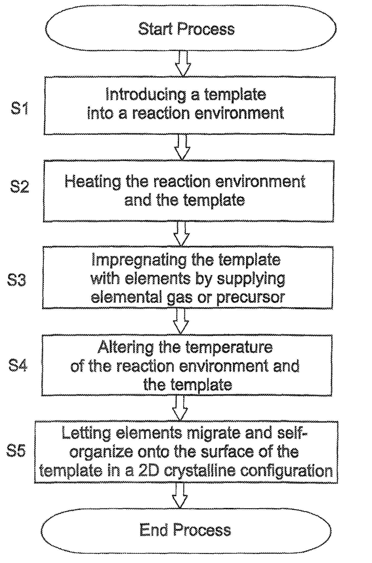
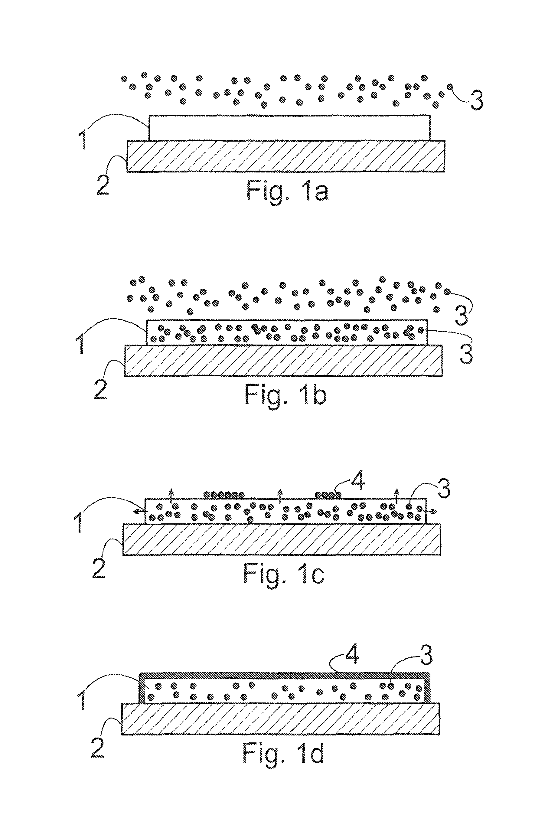
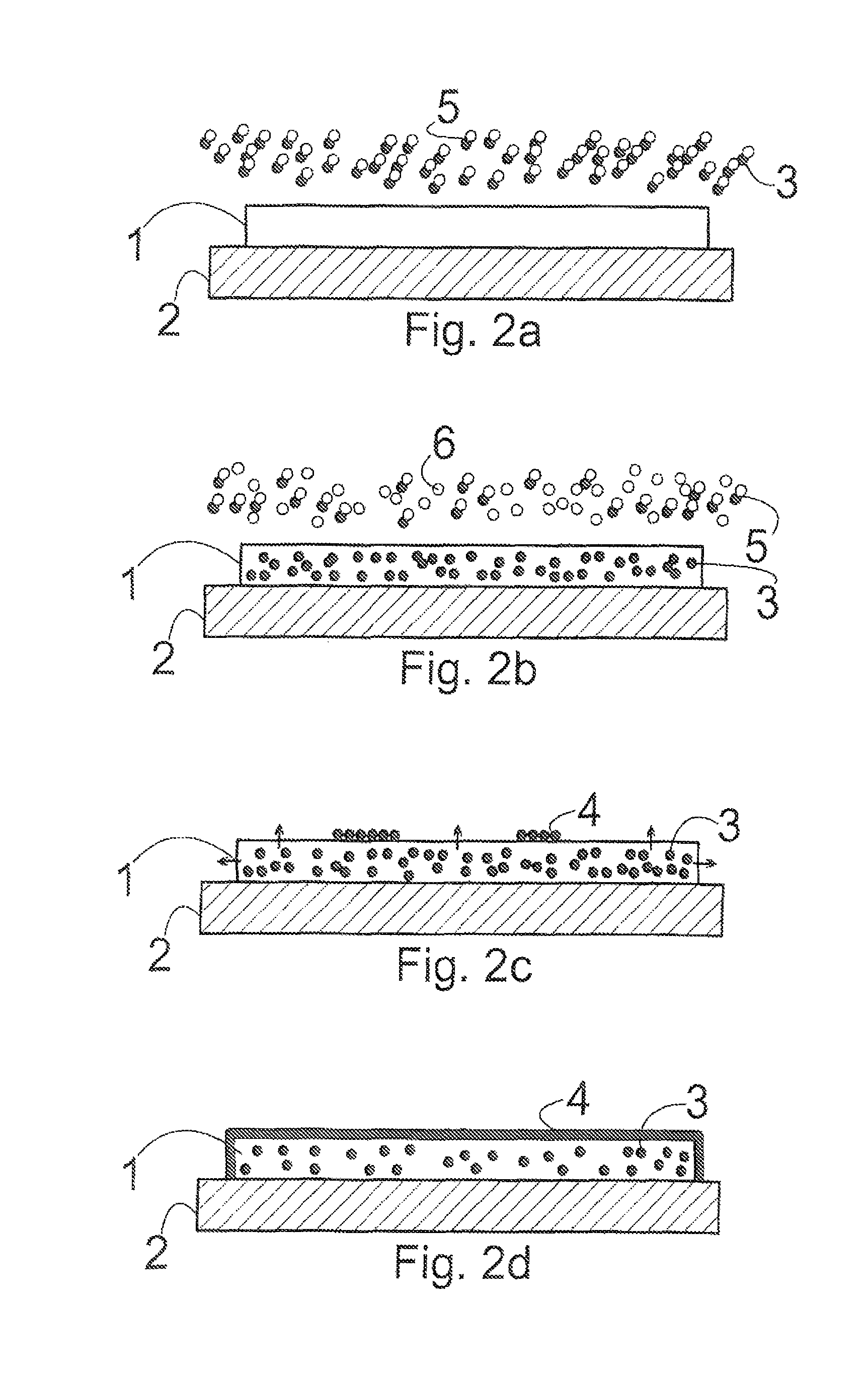
[0054]Example 1 pertains to graphene nanoribbons synthesized from a gaseous carbon precursor on an iron template 1, according to one embodiment of the invention. In this example, iron is deposited on a substrate 2 by, for instance, sputtering in the desired pattern, for instance in a ribbon. The iron deposit template 1 on the substrate 2 is then placed in a reaction environment into which a gaseous carbon source, CO precursor in this case (an organic precursor or a hydrocarbon, such as alcohol vapor or methane are also suitable), is introduced. The conditions in the reaction environment are then modified by elevating the temperature such that the carbon element 3 from the carbon precursor is released from the precursor 5 and diffuses into the iron ribbon template 1 for a period of time, such that the template 1 becomes saturated with carbon. The carbon (the element 3) can be released in the gas phase and then diffuse or migrate into the iron deposit as would be the case for, for ins...


PUM

PropertyMeasurementUnit
thickaaaaaaaaaa
thickaaaaaaaaaa
thickaaaaaaaaaa

Abstract

A method for fabricating crystalline surface structures (4) on a template (1). The method comprises the steps of providing a template (1) into a reaction environment, wherein one or more elements (3) required for the formation of the crystalline surface structure (4) are contained within the template (1); heating the template (1) inside the reaction environment to increase the mobility of the element (3) within the template (1), and to increase the surface diffusion length of the element (3) on the template-environment interface; and activating the template (1) by altering the conditions within the reaction environment, to make the mobile element (3) slowly migrate towards the template-environment interface and to make the element (3) organize on the surface of the template (1) as a crystalline structure (4).

Description

FIELD OF THE INVENTION[0001]The present invention relates to film growth technology. Specifically the present invention relates crystalline surface structures and to methods for fabricating crystalline structures on the surface of a template.BACKGROUND OF THE INVENTION[0002]Examples of so called monolayer crystalline surface (MCS) structures include essentially two-dimensional lattices of carbon (e.g. graphene), nitrogen and boron. When many parallel monolayers are present, such structures constitute a bulk material (as opposed to a film). Layered structures of 1 to 10 layers of essentially coplanar MCS-structures can be termed as few-layered crystalline surface (FCS) structures and they can still be termed films. Bulk or many-layered material containing tens of layers of essentially coplanar FCS-structures, when containing carbon, are termed graphite. FCS-structures can be distinguished from bulk also in that quantum effects are still important when the number of layers is small.[0...

Claims


Application Information

Patent Timeline
Patent Type & Authority Patents(United States)
IPC IPC(8): C01B31/00C23C8/80B82Y30/00B82Y40/00C01B31/04C23C8/00H01L21/02C23C8/22C23C8/40C23C8/08C23C8/02
CPCC23C8/22B82Y30/00B82Y40/00C01B31/0453C23C8/00C23C8/02C23C8/08C23C8/40C23C8/80H01L21/0254H01L21/02439H01L21/02491H01L21/02527H01L21/02612H01L21/02658C01B2204/02C01B2204/04C01B2204/06C01B32/186B82B3/00C01B32/194C01B32/40
Inventor BROWN, DAVID P.PFALER, JAN VON
Owner CANATU OY
Why Eureka
Try Eureka