Non-volatile memory cell

a memory cell, non-volatile technology, applied in the direction of electrical equipment, semiconductor devices, instruments, etc., can solve the problems of poor endurance of non-volatile memory cells in the prior ar

Active Publication Date: 2016-11-15
AMIC TECH TAIWAN
View PDF7 Cites 1 Cited by
  • Summary
  • Abstract
  • Description
  • Claims
  • Application Information

AI Technical Summary

Problems solved by technology

The non-volatile memory cells in the prior art suffer from the poor endurance.

Method used


Image

  • Non-volatile memory cell
  • Non-volatile memory cell
  • Non-volatile memory cell

Examples


Embodiment Construction

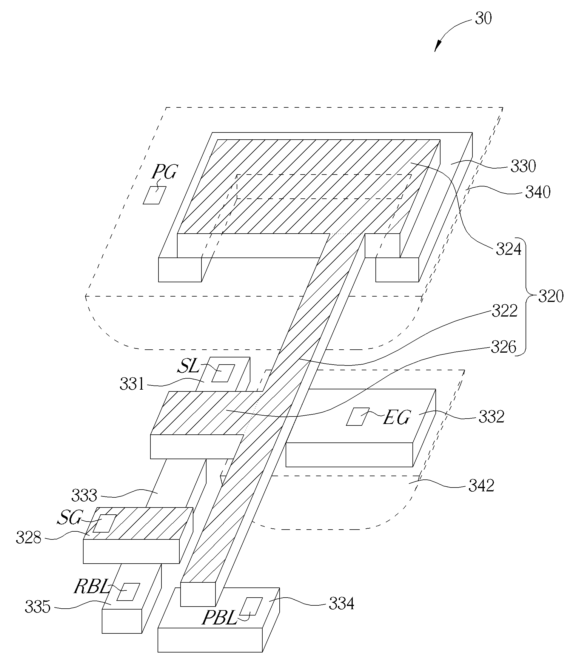
[0024]The non-volatile memory cell in the present invention is fabricated by a logic-based complementary metal oxide semiconductor (CMOS) process. The logic-based CMOS process is known in the art. In short, in a fabrication perspective, the logic-based CMOS process implants an active region in an electron well, and forms an insulation layer and a conductive layer in the electron well above the active region. In a circuit layout perspective, the active region is under the insulation layer and the conductive layer, and the electron well is disposed under the active region. Therefore, in the following description and in the claims, “over” and “under” represent relative positions of different layers in circuit layout. For example, “the electron well is disposed under the active region” represents the active region is implanted in the electron well, and “the insulation layer and the conductive layer is disposed over the active region” or “the active region is disposed under the insulatio...


PUM


Abstract

A non-volatile memory cell includes a tunneling part; a coupling device; a read transistor; a first select transistor connected to the read transistor forming a read path with the read transistor in a read mode; an erase tunneling structure forming a tunneling ejection path in an erase mode; and a program tunneling structure forming a tunneling injection path in an program mode; wherein the read path is different from the tunneling ejection path and the tunneling injection path.

Description

BACKGROUND OF THE INVENTION[0001]1. Field of the Invention[0002]The present invention relates to a non-volatile memory cell, and more particularly, to a non-volatile memory cell with enhanced endurance.[0003]2. Description of the Prior Art[0004]Non-volatile memory is a kind of memory which is capable of storing data without power supply. Common non-volatile memories include magnetic memory devices, CD-ROM, flash memory, etc. In general, the non-volatile memory is fabricated by a logic based complementary metal oxide semiconductor (CMOS) process. Each non-volatile memory cell of the non-volatile memory may operate in a read mode, a program mode and an erase mode.[0005]The non-volatile memory cells in the prior art suffer from the poor endurance. Specifically, when the non-volatile memory cell operates in a program / erase mode, a tunneling effect is produced on a floating gate of the non-volatile memory cell by apply proper bias voltages to perform a program / erase operation. After the ...

Claims


Application Information

Patent Timeline
Patent Type & Authority Patents(United States)
IPC IPC(8): H01L27/115G11C16/14H01L29/788G11C16/02
CPCH01L29/7883G11C16/02H01L27/1157H01L27/11524H01L27/11529H01L27/11573H01L29/7881H10B41/35H10B41/70H10B41/41H10B43/35H10B43/40
Inventor LU, HSIAO-HUAKUO, CHIH-MINGCHANG, CHIH-LUNG
Owner AMIC TECH TAIWAN
Why Eureka
Try Eureka