Single-polycrystalline EEPROM switch unit structure

A technology of switching units and switching tubes, which is applied to electrical components, static memory, instruments, etc., can solve the problems of high repair and adjustment cost, low repair and adjustment yield, and inability to realize repeated repair and adjustment, and achieve high repair and adjustment yield, Trimming Flexible, repeatable, and precise trimming effects

Pending Publication Date: 2022-04-05
58TH RES INST OF CETC
View PDF0 Cites 0 Cited by
  • Summary
  • Abstract
  • Description
  • Claims
  • Application Information

AI Technical Summary

Problems solved by technology

[0003] In analog integrated circuits, commonly used trimming methods include physical trimming methods such as fuse trimming and laser trimming. These methods have high trimming costs, low trimming yields, and cannot achieve repeated trimming

Method used


Image

  • Single-polycrystalline EEPROM switch unit structure
  • Single-polycrystalline EEPROM switch unit structure
  • Single-polycrystalline EEPROM switch unit structure

Examples


Embodiment Construction

[0025] The structure of a single-polycrystalline EEPROM switch unit proposed by the present invention will be further described in detail below in conjunction with the accompanying drawings and specific embodiments. Advantages and features of the present invention will be apparent from the following description and claims. It should be noted that all the drawings are in a very simplified form and use imprecise scales, and are only used to facilitate and clearly assist the purpose of illustrating the embodiments of the present invention.

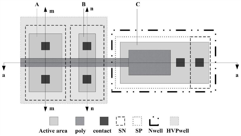
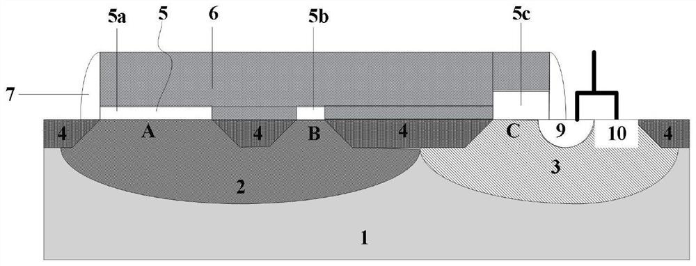
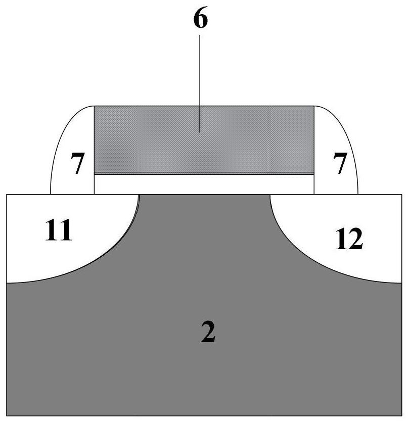
[0026] The invention provides a single polycrystalline EEPROM switch unit structure, its hierarchical structure is as follows figure 1 As shown, it can play the role of repeatable trimming in power management and digital-analog mixed-signal circuits. It has the characteristics of simple process, complete compatibility with CMOS process, low manufacturing cost, and strong portability. It can be widely used in power supply Management circuit o...


PUM

PropertyMeasurementUnit
thicknessaaaaaaaaaa

Abstract

The invention discloses a single-polycrystalline EEPROM (Electrically Erasable Programmable Read-Only Memory) switch unit structure, which belongs to the field of microelectronic devices and comprises a p-type Si substrate, a shallow trench isolation (STI), a gate oxide layer, a polycrystalline layer and a liner. A high-voltage p well and a high-voltage n well are formed on the p-type Si substrate; the surface of the p-type Si substrate is divided into three areas, namely a switch tube area, a programming tube area and a control gate area, by a plurality of STIs (shallow trench isolators); a tunneling injection layer is formed on the surface of the programming tube region through n-type ion doping; the gate oxide layer is located on the surface of the p-type Si substrate; the polycrystalline layer is deposited on the surface of the gate oxide layer and covers the switch tube region, the programming tube region, the control gate region and the shallow trench isolation STI; the pads are located on the two sides of the polycrystalline layer, and an N + ion implantation layer and a P + ion implantation layer are formed on the p-type Si substrate through the gate self-alignment process of the pads. According to the invention, a repeated and accurate trimming function can be realized; the method has the prominent advantages of flexible trimming, high trimming yield, low process cost, easy realization of process transplantation and the like.

Description

technical field [0001] The invention relates to the technical field of microelectronic devices, in particular to a single-polycrystalline EEPROM switch unit structure. Background technique [0002] In power management, digital-analog, and analog signal processing circuits, the use of trimming technology is the mainstream method to combat process fluctuations and improve the accuracy of circuit processing signals. [0003] In analog integrated circuits, commonly used trimming methods include physical trimming methods such as fuse trimming and laser trimming. These methods have high trimming costs, low trimming yields, and cannot achieve repeated trimming. Contents of the invention [0004] The purpose of the present invention is to provide a single polycrystalline EEPROM switch unit structure to solve the problems in the background technology. [0005] In order to solve the above-mentioned technical problems, the present invention provides a single-polycrystalline EEPROM s...

Claims


Application Information

Patent Timeline
Patent Type & Authority Applications(China)
IPC IPC(8): H01L27/11526G11C16/04G11C16/12
Inventor 宋思德葛江晖郑若成贺琪刘国柱徐蓓蕾
Owner 58TH RES INST OF CETC
Why Eureka
Try Eureka