Thin-film transistor element, method for manufacturing same, and display device
a technology of thin film transistors and elements, applied in the direction of transistors, semiconductor devices, electrical devices, etc., can solve the problems of oxide semiconductor properties likely to degrade, and achieve the effect of suppressing the peak of the mobility curv
- Summary
- Abstract
- Description
- Claims
- Application Information
AI Technical Summary
Benefits of technology
Problems solved by technology
Method used
Image

Examples
embodiment 1
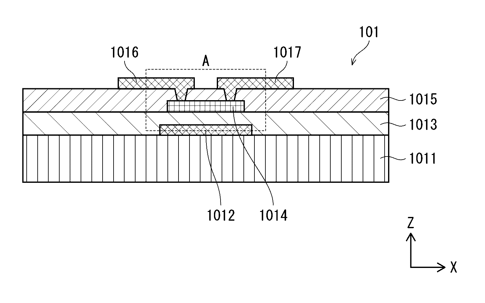
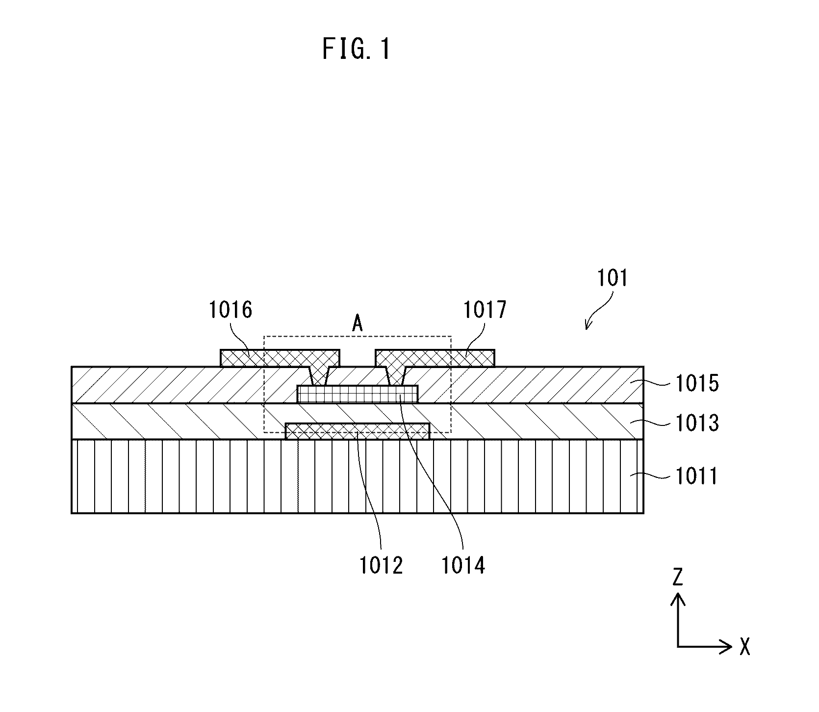
[0080]The following describes a TFT element 101 of the inverted-staggered type and of the channel protection type according to Embodiment 1 of the present invention.
[0081]1. Cross-Sectional Configuration of TFT Element 101
[0082]The following describes a cross-sectional configuration of the TFT element 101 with reference to FIG. 1.
[0083]As shown in FIG. 1, in the TFT element 101, a gate electrode 1012 is disposed on a substrate 1011. Furthermore, a gate insulation layer 1013 is disposed to cover the gate electrode 1012.
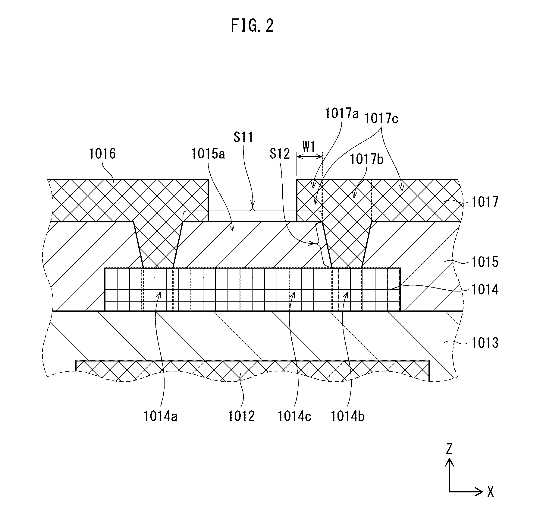
[0084]Also, a channel layer 1014 is disposed on the gate insulation layer 1013, i.e., above the gate electrode 1012, and is not adjacent to the gate electrode 1012. Furthermore, a channel protection layer 1015 is disposed to cover the channel layer 1014. A portion of the channel protection layer 1015 on the channel layer 1014 is provided with a contact hole, and a portion of the channel layer 1014 is exposed from the channel protection layer 1015.
[0085]Also, a source e...
embodiment 2
[0159]The following describes an organic EL display device 2 according to Embodiment 2 of the present invention. The present embodiment is an example in which the TFT element 101 according to Embodiment 1 is adopted in the organic EL display device 2.
[0160]1. Overall Configuration of Organic EL Display Device 2
[0161]The following describes the configuration of the organic EL display device 2 according to the present embodiment with reference to FIG. 10.
[0162]As shown in FIG. 10, the organic EL display device 2 includes an organic EL display panel 20 and a drive control unit 30 connected therewith.
[0163]The organic EL display panel 20 is a panel utilizing the electric-field light-emitting phenomenon of organic material. The organic EL display panel 20 has a plurality of sub pixels 20a (not shown in FIG. 10) corresponding to luminescent colors such as red, green, and blue, and they are arranged in a matrix. The drive control unit 30 includes four drive circuits, namely drive circuits ...
embodiment 3
[0226]The following describes a TFT element 301 according to Embodiment 3 as an aspect of the present invention. Note that, of the TFT element 301, the same parts as in the TFT element 101 are labelled using the same reference signs, and a description thereof is omitted.
[0227]1. Configuration
[0228]FIG. 13 is a schematic cross-sectional diagram that magnifies a portion of the TFT element 301, and that corresponds to FIG. 2 for the TFT element 101. Like the TFT element 101, the TFT element 301 is a TFT element of the inverted-staggered type and of the channel protection type. The TFT element 301 includes channel protection layer 3015 and a drain electrode 3017 as elements different from the TFT element 101.
[0229]The channel protection layer 3015 covers the channel layer 1014 except for the source contact region 1014a and the drain contact region 1014b so that the source contact region 1014a and the drain contact region 1014b are exposed. Consequently, the surface of the channel protec...
PUM
 Abstract
Description
Claims
Application Information