Method for growing graphene on surface of gate electrode and method for growing graphene on surface of source/drain surface

a technology of gate electrodes and graphene, which is applied in the field of display technology, can solve problems affecting the electrical performance of the entire tft device, and achieve the effects of simple manufacturing process, improved vapor deposition process, and improved electrical performan

Active Publication Date: 2017-01-10
TCL CHINA STAR OPTOELECTRONICS TECH CO LTD
View PDF6 Cites 19 Cited by
  • Summary
  • Abstract
  • Description
  • Claims
  • Application Information

AI Technical Summary

Benefits of technology

[0030]The efficacy of the present invention is that the present invention provides a method for growing graphene on a surface of a gate electrode and a method for growing graphene on a surface of a source / drain electrode, in which a low-temperature plasma enhanced vapor deposition process is adopted to grow a graphene film, of which a film thickness is controllable, on a gate electrode or a source / drain electrode that contains copper, and completely coincides with a pattern of the gate electrode or the source / drain electrode. The manufacturing temperature of graphene is relatively low so that it is possible not to damage the structure of a thin-film transistor to the greatest extents and the supply of carbon sources that is used wide, having low cost and a simple manufacturing process, where existing PECVD facility of a thin-film transistor manufacturing line can be used without additional expense. The gate electrode or the source / drain electrode is covered with graphene and is prevented from contact with moisture and oxygen thereby overcoming the problem of a conventional TFT manufacturing process that a gate electrode or a source / drain electrode that contains copper is readily susceptible to oxidization. Further, the high electrical conductivity of graphene makes it possible not to affect the electrical performance of the entire device.

Problems solved by technology

In the conventional copper processes, to serve as the gate electrode and the source / drain electrode, copper must often be exposed for the performance of the subsequent processes and would be readily susceptible to oxidization in the subsequent high-temperature and high-humidity processes that leads to a non-conductive isolation layer on the surface of the copper thereby affecting the electrical performance of the entire TFT device.

Method used


Image

  • Method for growing graphene on surface of gate electrode and method for growing graphene on surface of source/drain surface
  • Method for growing graphene on surface of gate electrode and method for growing graphene on surface of source/drain surface
  • Method for growing graphene on surface of gate electrode and method for growing graphene on surface of source/drain surface

Examples


Embodiment Construction

[0039]To further expound the technical solution adopted in the present invention and the advantages thereof, a detailed description is given to a preferred embodiment of the present invention and the attached drawings.

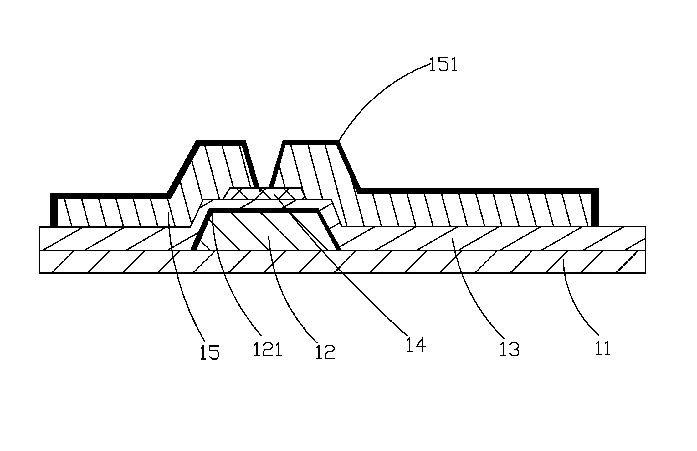
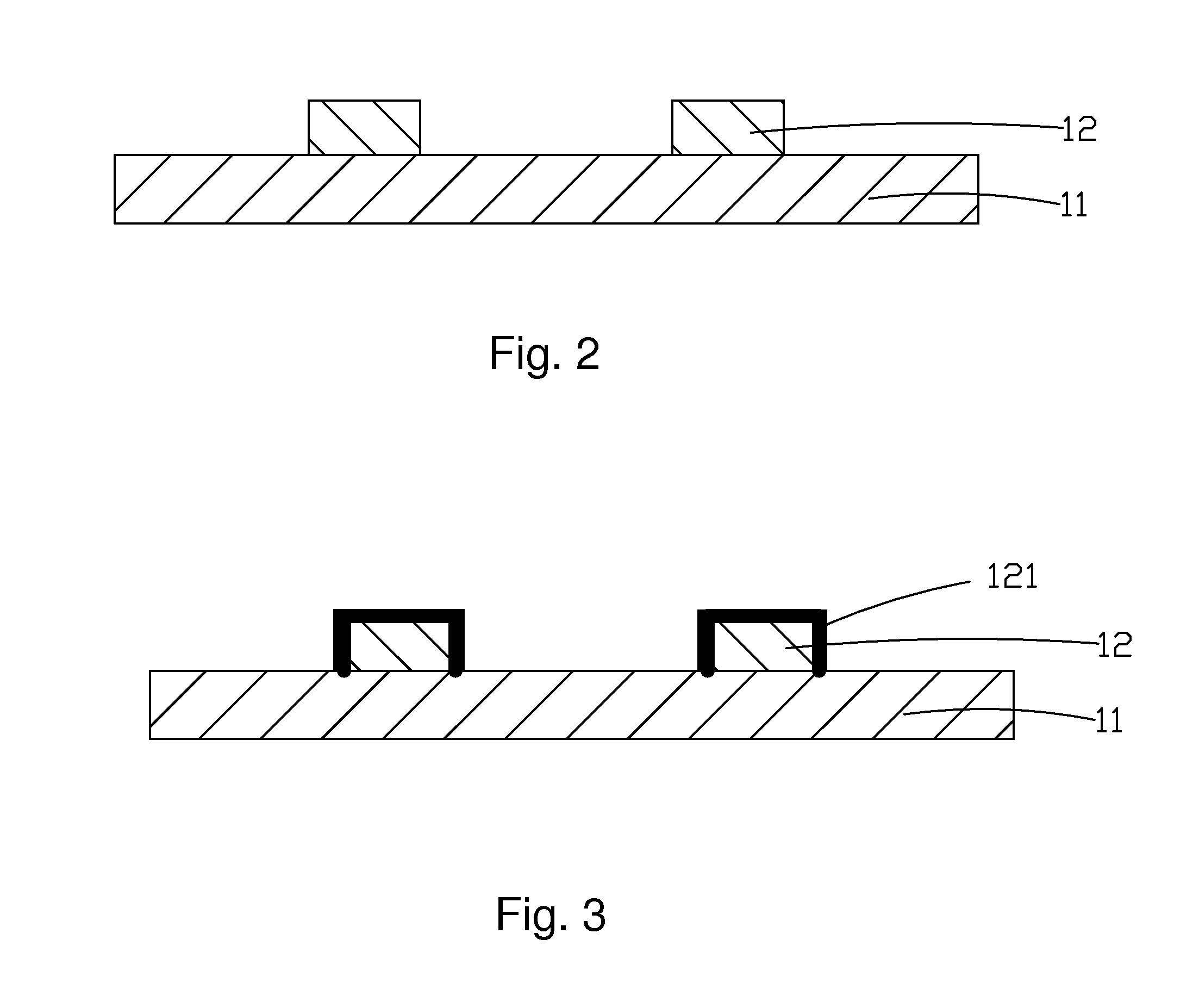
[0040]Taking into consideration the requirement for temperature in the manufacture of a thin-film transistor liquid crystal display (TFT-LCD), the present invention employs a low-temperature plasma enhanced chemical vapor deposition (PECVD) to grow a film-thickness-controllable graphene film on a surface of a gate electrode or a source / drain electrode that contains copper and allows graphene to grow according to a pattern of the gate electrode or source / drain electrode. Specifically speaking, in the entire process of reaction, copper contained in the gate electrode or the source / drain electrode plays a role of catalyst so that carbon-contained precursors decompose on a surface of copper to form nuclei and get crystalized, while such a reaction does not occur in other a...


PUM

PropertyMeasurementUnit
pressureaaaaaaaaaa
temperatureaaaaaaaaaa
pressureaaaaaaaaaa

Abstract

The present invention provides a method for growing graphene on a surface of a gate electrode and a method for growing graphene on a surface of a source/drain electrode, in which a low-temperature plasma enhanced vapor deposition process is adopted to grow a graphene film, of which a film thickness is controllable, on a gate electrode or a source/drain electrode that contains copper, and completely coincides with a pattern of the gate electrode or the source/drain electrode. The manufacturing temperature of graphene is relatively low so that it is possible not to damage the structure of a thin-film transistor to the greatest extents and the supply of carbon sources that is used wide, having low cost and a simple manufacturing process, where existing PECVD facility of a thin-film transistor manufacturing line can be used without additional expense. The gate electrode or the source/drain electrode is covered with graphene and is prevented from contact with moisture and oxygen thereby overcoming the problem of a conventional TFT manufacturing process that a gate electrode or a source/drain electrode that contains copper is readily susceptible to oxidization. Further, the high electrical conductivity of graphene makes it possible not to affect the electrical performance of the entire device.

Description

BACKGROUND OF THE INVENTION[0001]1. Field of the Invention[0002]The present invention relates to the field of display technology, and in particular to a method for growing graphene on a surface of a gate electrode and a method for growing graphene on a surface of a source / drain electrode.[0003]2. The Related Arts[0004]In the field of display technology, flat panel displays, such as a liquid crystal display (LCD) and an organic light-emitting diode (OLED), have gradually taken the place of a cathode ray tube (CRT) display device and are widely used in liquid crystal televisions, mobile phones, personal digital assistants, digital cameras, computer displays, and notebook computer screens.[0005]A display panel is an important constituent component of the LCD and OLED. The display panel of the LED and the display panel of the OLED both comprise a thin-film transistor (TFT) array substrate. Taking an LCD display panel as an example, it is made up of a TFT array substrate, a color filter ...

Claims


Application Information

Patent Timeline
Patent Type & Authority Patents(United States)
IPC IPC(8): H01L21/28H01L21/285
CPCH01L21/28247H01L21/28506H01L29/1606H01L29/41733H01L29/42384H01L29/4908H01L29/45
Inventor HU, TAO
Owner TCL CHINA STAR OPTOELECTRONICS TECH CO LTD
Why Eureka
Try Eureka