Method of manufacturing a silicon dioxide layer

a manufacturing method and silicon dioxide technology, applied in the direction of liquid surface applicators, coatings, chemical vapor deposition coatings, etc., can solve the problems of lack of reproducibility of process, lack of uniformity of resulting layer, low process throughput, etc., to eliminate the use of chemical and mechanical polishing and superior electrical features

Active Publication Date: 2007-06-14
S O I TEC SILICON ON INSULATOR THECHNOLOGIES +1
View PDF18 Cites 5 Cited by
  • Summary
  • Abstract
  • Description
  • Claims
  • Application Information

AI Technical Summary

Benefits of technology

[0012] The present invention now overcome the above-mentioned drawbacks and in particular eliminates the use of chemical and mechanical polishing. Consequently, the invention aims to improve the LPCVD TEOS deposition process, in order to obtain a high quality silicon dioxide layer 2 which meets substrate direct bonding criteria in terms of surface roughness, uniformity and particle density and which can be used as buried oxide layer. In addition, the invention also provides an interface with superior electrical features.

Problems solved by technology

In the above-mentioned process, the polishing step of FIG. 1B presents numerous drawbacks such as the lack of uniformity of the resulting layer 2, the lack of reproducibility of the process and the low throughput of the process.
Further, this additional step increases the manufacturing cost of each substrate or wafer.

Method used


Image

  • Method of manufacturing a silicon dioxide layer
  • Method of manufacturing a silicon dioxide layer
  • Method of manufacturing a silicon dioxide layer

Examples


Embodiment Construction

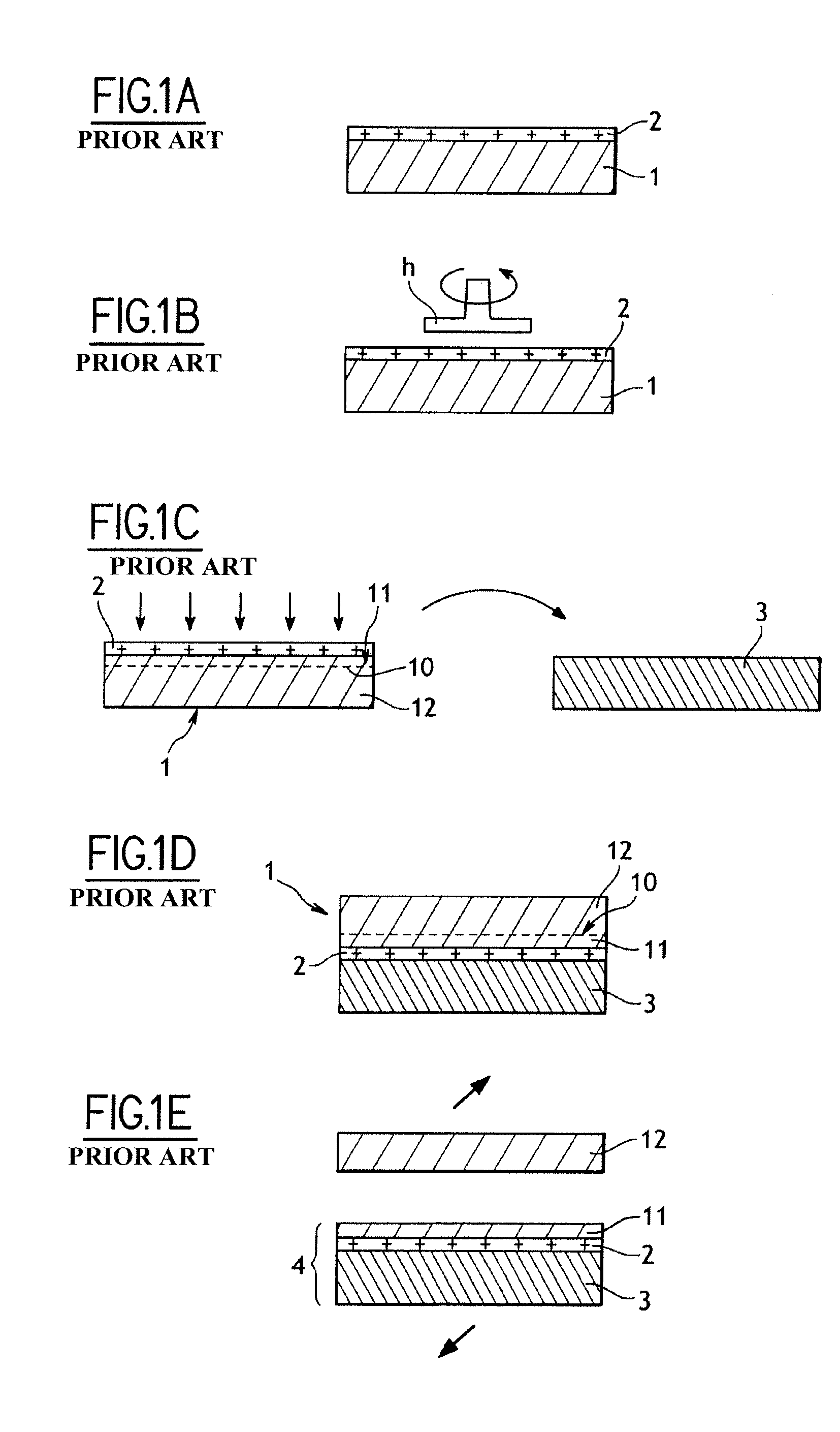
[0028] According to the invention, the silicon dioxide deposition step of FIG. 1A is improved as mentioned above, but the method of the present invention.

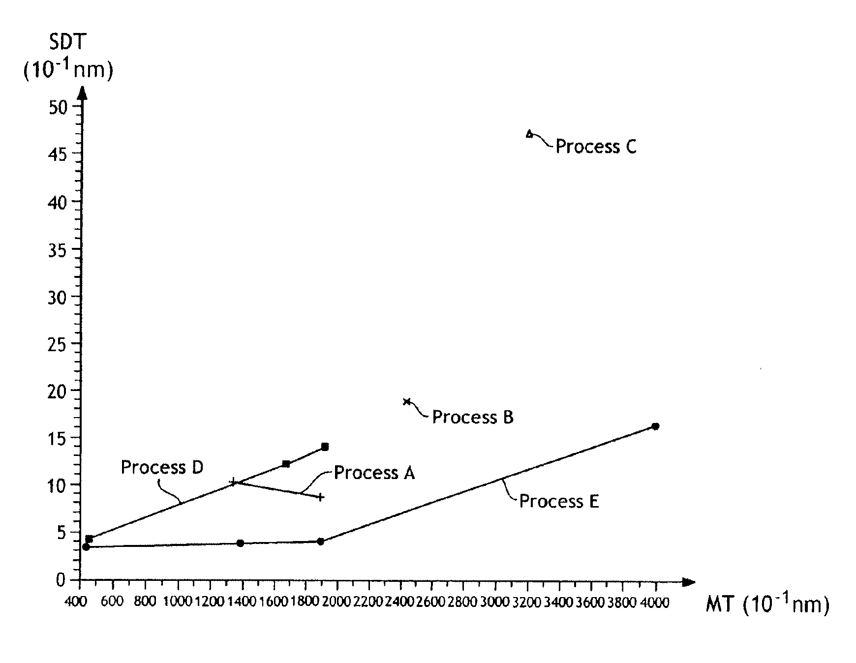
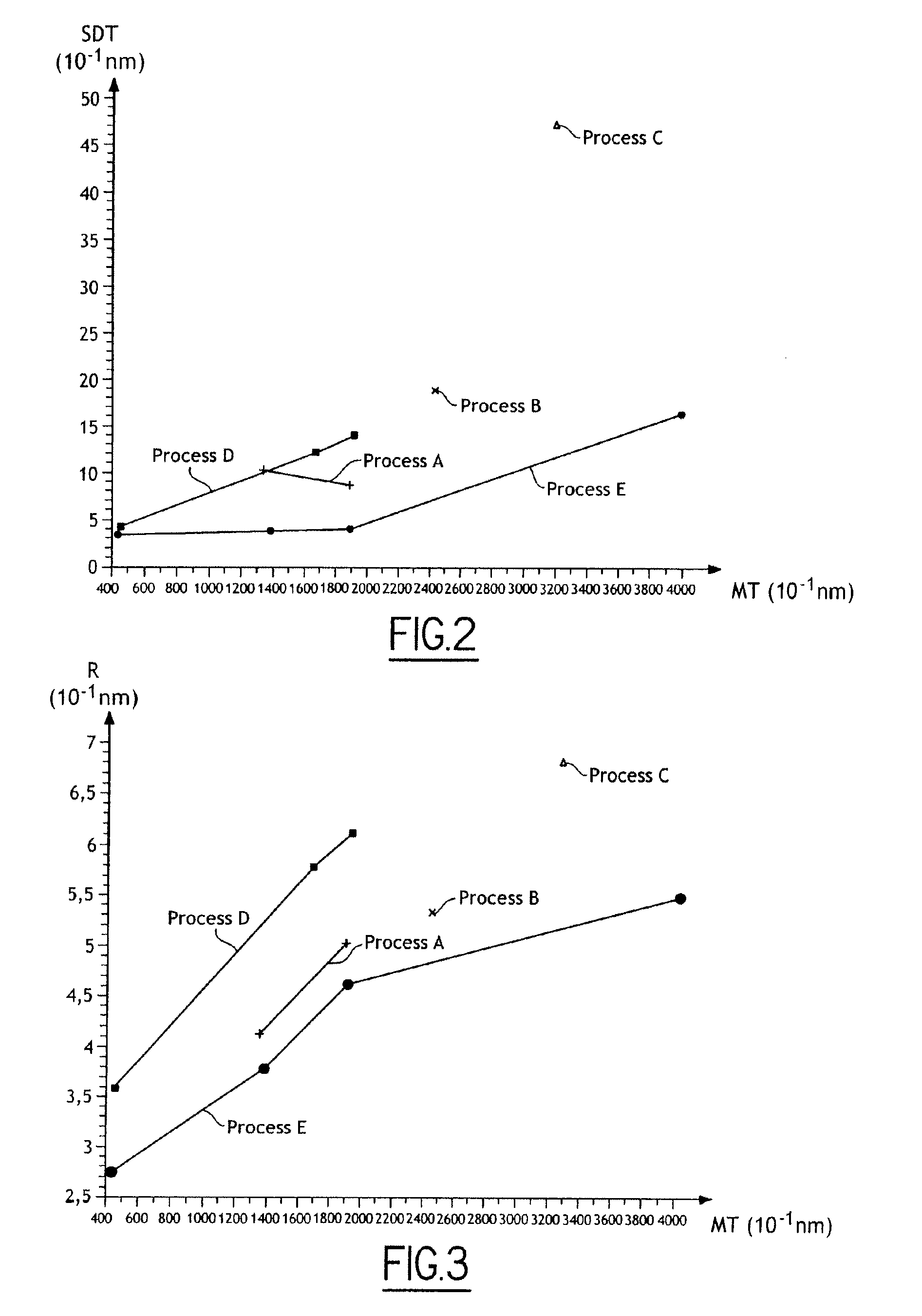
[0029] It has now been discovered that the roughness of a silicon dioxide layer obtained by a “LPCVD TEOS” deposition process may be reduced by the use of a flow of a diluent gas simultaneously with a flow of TEOS during the deposition process. The diluent gas is preferably nitrogen but it can be any other gas that is not reactive with TEOS, of which argon (Ar) and helium (He) are non-limiting examples. Alternatively, any mixture of such non-reactive gases can be used.

[0030] The methods for determining the best operating conditions will now be described. Silicon dioxide deposition was performed by a low pressure vapour chemical deposition (LPVCD) process, which includes introducing a batch of source substrates inside the process chamber of a LPCVD reactor, and introducing gaseous flow of different chemical reactants, at elevated ...


PUM

PropertyMeasurementUnit
temperatureaaaaaaaaaa

Abstract

The invention relates to a of manufacturing a silicon dioxide layer of low roughness, that includes depositing a layer of silicon dioxide over a substrate by a low pressure chemical vapour deposition (LPCVD) process, the deposition process employing simultaneously a flow of tetraethylorthosilicate (TEOS) as the source material for the film deposition and a flow of a diluant gas that it not reactive with TEOS, so that the diluant gas/TEOS flow ratio is between 0.5 and 100; and annealing the silicon dioxide layer at a temperature between 600° C. and 1200° C., for a duration between 10 minutes and 6 hours.

Description

CROSS-REFERENCE TO RELATED APPLICATIONS [0001] This application is a continuation of International application PCT / EP2004 / 011616 filed Sep. 16, 2004, the entire content of which is expressly ioncorporated herein by reference thereto.BACKGROUND ART [0002] The invention relates to a method of manufacturing a silicon dioxide layer of low roughness deposited on a substrate and to a method of manufacturing a composite substrate or wafer including such silicon dioxide layer as buried layer, in particular for applications in the fields of optics, optoelectronics or electronics. [0003]FIGS. 1A to 1E illustrate the different steps of a prior art process employed for manufacturing such a composite substrate. [0004] As can be seen on FIG. 1A, a silicon dioxide layer 2 is firstly deposited on a bulk substrate 1 termed the “source substrate”, because it is used to provide the material that will constitute later the top layer of the composite substrate. In view of the kind of composite substrate ...

Claims


Application Information

Patent Timeline
Patent Type & Authority Applications(United States)
IPC IPC(8): H01L21/473
CPCC23C16/402H01L21/02164H01L21/02216H01L21/02271H01L21/31612
Inventor BOURDELLE, KONSTANTINDAVAL, NICOLASCAYREFOURCQ, IANVAN AERDE, STEVEN R.A.DE BLANK, MARINUS J.M.VAN DER JEUGD, CORNELIUS A.
Owner S O I TEC SILICON ON INSULATOR THECHNOLOGIES
Why Eureka
Try Eureka