
Methods for producing a thin film ferroelectric device using a two-step temperature process on an organic polymeric ferroelectric precursor material stacked between two conductive materials

a technology of ferroelectric precursor material and temperature process, which is applied in the direction of thermoelectric devices, solid-state devices, coatings, etc., can solve the problems of affecting the stable operation of the film, the current available processes, and the routine development of nano-size cracks on the pvdf film, so as to reduce the interfacial void or crack in the resulting material, reduce the interfacial void, and improve the durability of the ferroelectric film used

Inactive Publication Date: 2017-01-10
SABIC GLOBAL TECH BV
View PDF19 Cites 6 Cited by
  • Summary
  • Abstract
  • Description
  • Claims
  • Application Information

AI Technical Summary

Benefits of technology

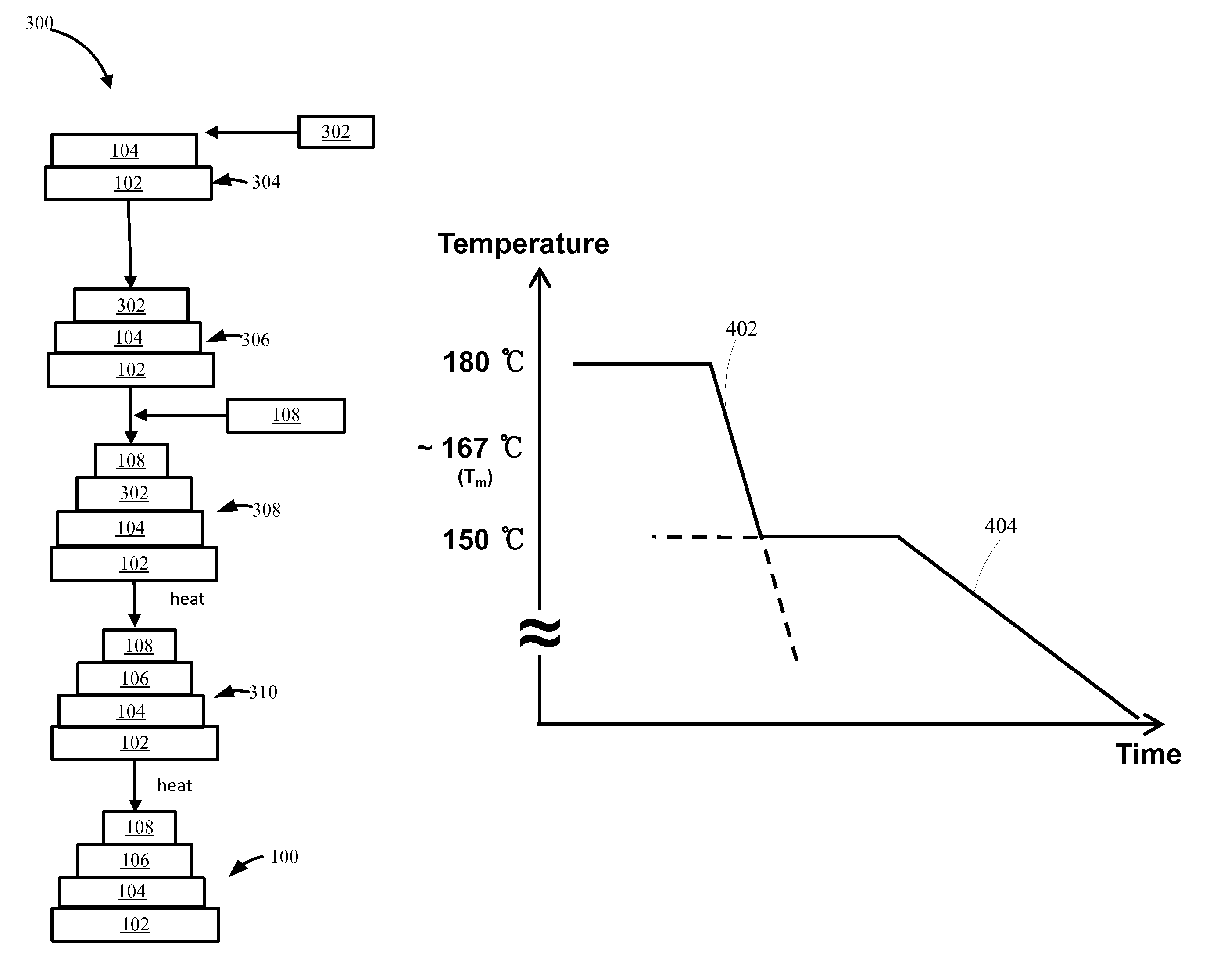
The patent describes a solution to poor durability of ferroelectric films used in memory devices. The solution involves a controlled thermal annealing process of the precursor material, which converts it into material with ferroelectric hysteresis properties. The process includes heating the material to a high temperature to induce a phase transition, and then cooling it to a lower temperature to enhance the material's density and reduce interfacial voids. This process can be performed after the electronic device is constructed and does not require additional mechanical stretching or temperature steps. The patent also mentions a technique for blending polymers to create a polymer blend, which can be used to produce the ferroelectric material. This process is simple and allows for the fabrication of efficient ferroelectric electronic devices.

Problems solved by technology

Two problems, however, continue to arise with the currently available processes.
Second, and also after annealing, nano-size cracks routinely develop on the PVDF film, which are detrimental to the film's stable operation under applied voltage.

Method used


Image

  • Methods for producing a thin film ferroelectric device using a two-step temperature process on an organic polymeric ferroelectric precursor material stacked between two conductive materials
  • Methods for producing a thin film ferroelectric device using a two-step temperature process on an organic polymeric ferroelectric precursor material stacked between two conductive materials
  • Methods for producing a thin film ferroelectric device using a two-step temperature process on an organic polymeric ferroelectric precursor material stacked between two conductive materials

Examples


example 1

Fabrication of Ferroelectric Device with 2-Step Temperature Process

[0096]A ferroelectric capacitor of the present invention was fabricated using a two-step temperature process using the following method.

[0097]Polymer Solution. A solution of PVDF in solvent was prepared by adding PVDF powder (Sigma Aldrich®, MW=534,000 g / mol) to dimethylformamide solvent (Sigma Aldrich®). The solution was filtered using a polytetrafluoroethylene filter (1 μm pore size). The PVDF solution was stirred and heated at 110° C. using a conventional hot-plate for about 20 min to completely dissolve the PVDF. This heating of the PVDF solution ensured that the spin-coated PVDF thin-films would be uniform.

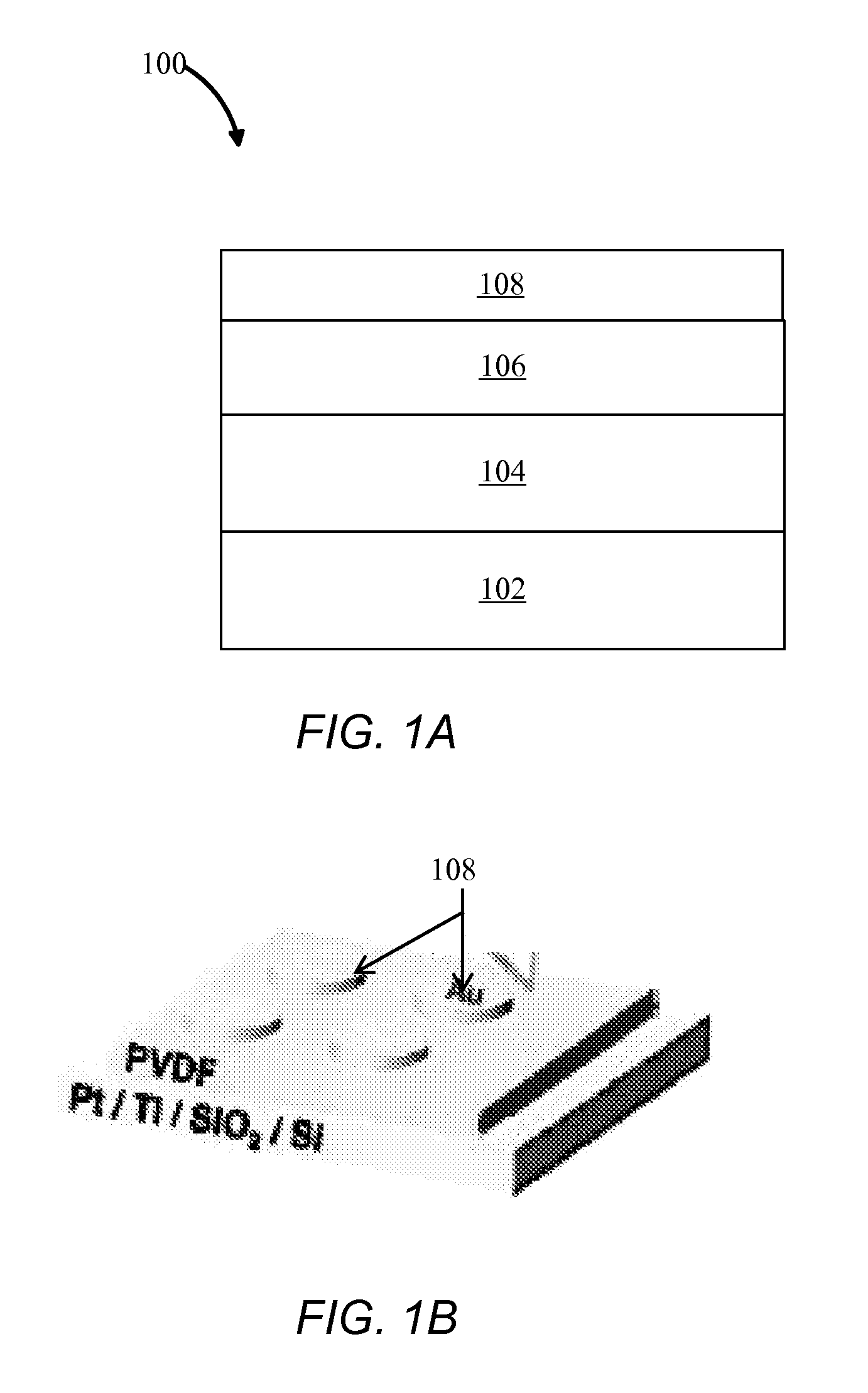
[0098]Ferroelectric Capacitor. A bottom electrode (25 nm-thick Pt (25 nm) / Ti (5 nm)) was sputter deposited on SiO2 (100 nm silicon). The bottom electrode and substrate was added to a spin coating apparatus. The hot polymer solution was deposited on the bottom electrode at a rate of 4000 rpm for 60 seconds to p...

example 2

Testing of Ferroelectric Devices of Example 1

[0099]Ferroelectric Hysteresis Properties During Annealing Process. Hysteresis loops for the ferroelectric devices of the present invention made in Example 1, were measured before and after the 2-step temperature process at a frequency of 100 Hz and are depicted in FIGS. 12A and 12B. FIG. 12A is a graphical depiction of the polarization (μC / cm2) versus electric field (MV / m) at 100 Hz for a ferroelectric device of the present invention before starting the 2-step temperature process. FIG. 12B is a graphical depiction of the polarization (μC / cm2) versus electric field (MV / m) at 100 Hz for a ferroelectric capacitor of the present invention after the two step temperature process. Comparing FIG. 12A to FIG. 12B, the hysteresis loop in FIG. 12B was more defined than for the hysteresis for the ferroelectric material in FIG. 12A, and thus demonstrating an improvement of the hysteresis properties of the ferroelectric material due to the two-step te...


PUM

PropertyMeasurementUnit
temperatureaaaaaaaaaa

Abstract

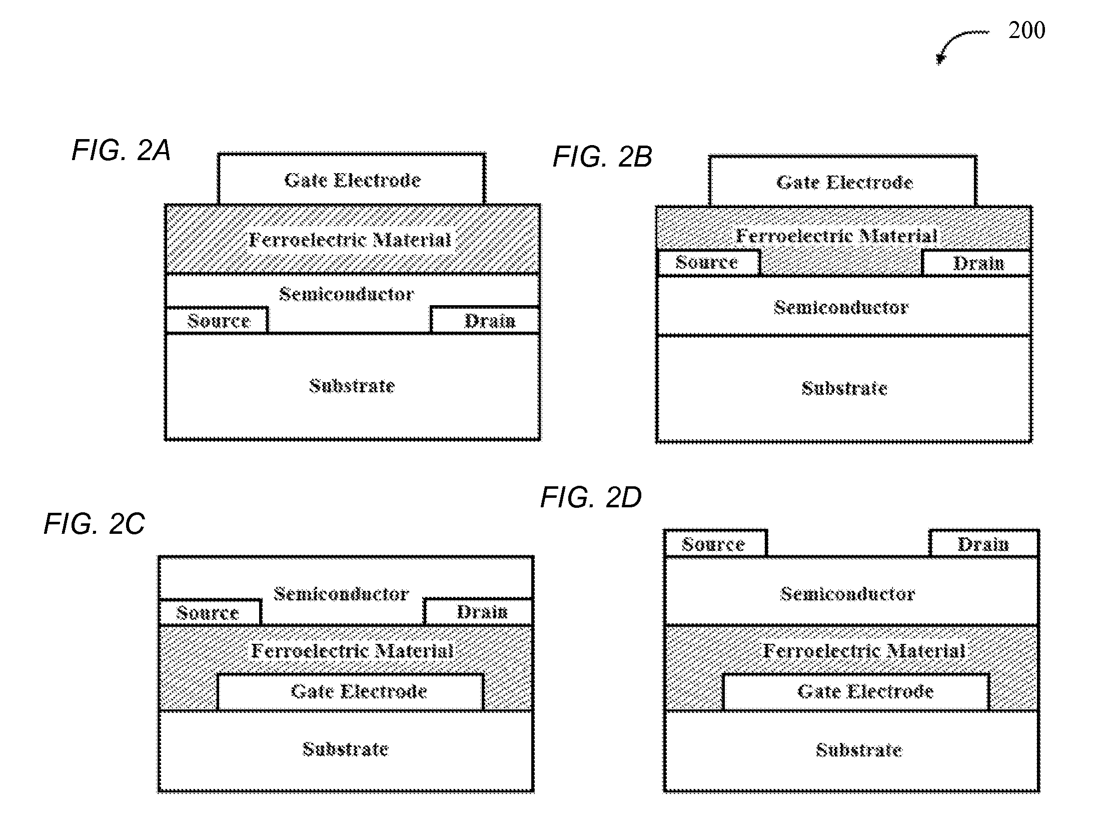
Methods for producing ferroelectric device are described. A method includes positioning an organic polymeric ferroelectric layer between two conductive materials to form a stack. The stack can be subjected to a 2-step heat treating process. The first heat treating step transforms the organic polymeric ferroelectric precursor to a ferroelectric material having ferroelectric hysteresis properties, and the second heat treating step densities the ferroelectric material to obtain the ferroelectric device. The thin film ferroelectric device can include a thin film ferroelectric capacitor, a thin film ferroelectric transistor, or a thin film ferroelectric diode.

Description

CROSS REFERENCE TO RELATED APPLICATIONS[0001]This application is a national phase application under 35 U.S.C. §371 of International Application No. PCT / US2015 / 034126, filed Jun. 4, 2015, which claims benefit to U.S. Provisional Patent Application No. 62 / 047,787 titled “METHODS FOR PRODUCING A THIN FILM FERROELECTRIC DEVICE USING A TWO-STEP TEMPERATURE PROCESS” filed Sep. 9, 2014. The entire contents of each of the above-referenced disclosures are specifically incorporated herein by reference without disclaimer.BACKGROUND OF THE INVENTION[0002]A. Field of the Invention[0003]The present invention generally relates to a method of producing ferroelectric films (e.g., poly(vinylidene fluoride) (PVDF) based films) and memory devices through a controlled two-step thermal annealing process.[0004]B. Description of Related Art[0005]Memory systems are used for storage of data, program code, and / or other information in many electronic products, such as personal computer systems, embedded proces...

Claims


Application Information

Patent Timeline
Patent Type & Authority Patents(United States)
IPC IPC(8): H01L27/115C09D127/16H01L29/66H01L21/02H01L21/321H01L37/02H01L41/113H01L41/193H01L41/317H01L29/78H01L21/28H01L29/51H10N30/098H10N15/10H10N30/077H10N30/20H10N30/30H10N30/857
CPCH01L27/1159C09D127/16H01L21/02118H01L21/02282H01L21/28176H01L21/321H01L27/11507H01L29/516H01L29/6684H01L29/78391H01L37/025H01L41/1132H01L41/193H01L41/317H01L21/324H10N15/10H10N30/302H10N30/04H10N30/077H10N30/098H01L21/32056H10B53/30H10B51/30H10N15/15H10N30/857
Inventor PARK, JI HOONALSHAREEF, HUSAM N.ODEH, IHAB N.KHAN, MOHD A.
Owner SABIC GLOBAL TECH BV
Learn More