Light-emitting device

a technology of light-emitting devices and light-emitting components, which is applied in the direction of semiconductor devices, semiconductor/solid-state device details, electrical devices, etc., can solve the problems of mark not being recognized during visual recognition or digital recognition, and achieve the effect of reducing the amount of sulfur

Active Publication Date: 2017-01-31
NICHIA CORP
View PDF15 Cites 3 Cited by
  • Summary
  • Abstract
  • Description
  • Claims
  • Application Information

AI Technical Summary

Benefits of technology

[0008]According to embodiments of the invention, the difference in reflectivity between the support body and the insulation layer is larger than the difference in reflectivity between the support body and the recognition target portion, which increases the contrast ratio of the support body to an area where the recognition target portion exists, so that the position of the recognition target portion can be recognized easily independent of the difference in reflectivity between the support body and the wiring pattern. Accordingly, even in a case where a difference in reflectivity between the support body and the wiring patterns is small, various kinds of processing with visual recognitions or digital recognitions such as inspection, mounting and division can be smoothly performed through the use of the insulation layer that covers the recognition target portion. Therefore, it is possible to select combinations of the support body and the wiring patterns in which the difference in reflectivity between the support body and the wiring patterns is small while other aspect such as heat-dissipation and sulfur resistance is good.

Problems solved by technology

And thus, with such a combination of the substrate and the feeder patterns, the mark may not be recognized during visual recognition or digital recognition, even if other aspect of the combination such as heat-dissipation and sulfur resistance is good.

Method used


Image

  • Light-emitting device
  • Light-emitting device
  • Light-emitting device

Examples


first example

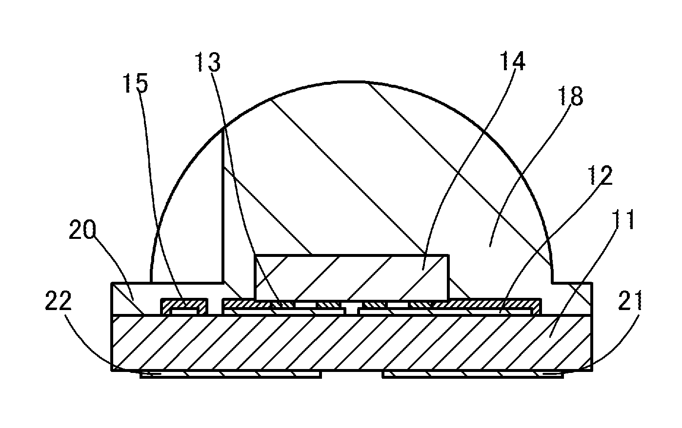
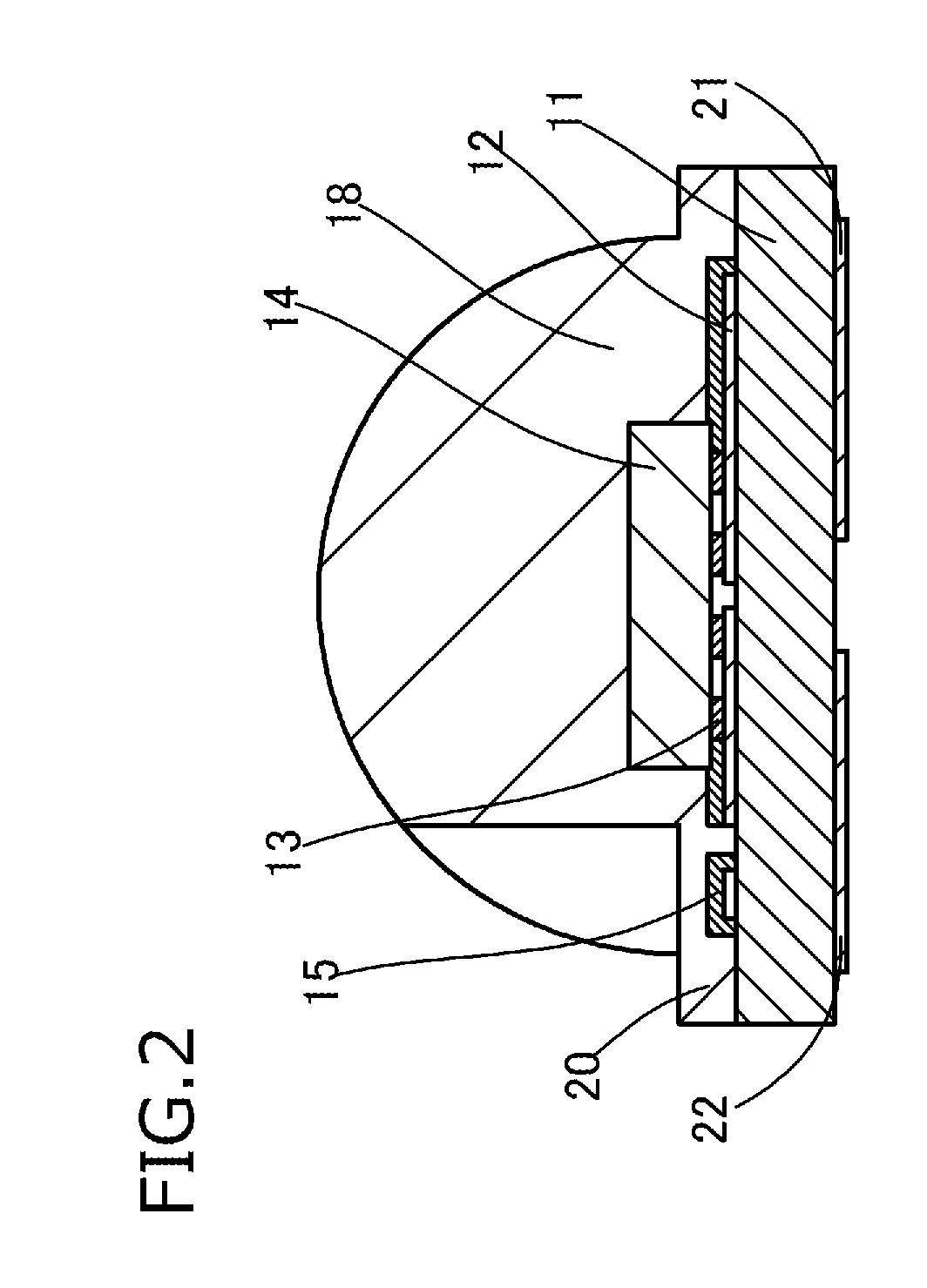
[0065]Next, a light-emitting device according to a first example will be described. The light-emitting device according to the first example is one example of the light-emitting device 100 according to the first embodiment, and aluminum nitride is used for the support body 11, and Au (gold) is used for the recognition target portion 19, and titanium oxide is used for the insulation layer 15. In the light-emitting device according to the first example, when it is assumed that the peak wavelength of the light emitted to the support body 11 and the insulation layer 15 during performing visual recognition or digital recognition is 450 nm, the reflectivity of aluminum nitride at the peak wavelength is 10 to 40%, and the reflectivity of Au is 30 to 60%, and the reflectivity of titanium oxide is 80 to 98%. Accordingly, in the light-emitting device according to the first example, the reflectivity of the recognition target portion 19 may become lower than the reflectivity of the support body...


PUM


Abstract

A light-emitting device includes a support body having a quadrangle planar shape, a wiring pattern on the support body, a light-emitting element on the wiring pattern, a recognition target portion on a corner portion of the support body, the recognition target portion including a conductive material, an insulation layer reflecting light emitted from the light-emitting element and covering a periphery of the recognition target portion, and a light-transmissive member including a lens portion covering the light-emitting element and a flange portion on a periphery of the lens portion and covering a portion of the recognition target portion that is covered with the insulation layer. The portion of the recognition target portion covered by the flange portion is arranged in a non-point symmetry around a center of the support body, and a difference in reflectivity between the support body and the insulation layer is larger than between the support body and the recognition target portion.

Description

CROSS-REFERENCE TO RELATED APPLICATION[0001]The present application claims priority to Japanese Patent Application No. 2014-242652, filed on Nov. 29, 2014, which is incorporated by reference in its entirety.BACKGROUND[0002]1. Field of the Invention[0003]The present invention relates to a light-emitting device.[0004]2. Description of Related Art[0005]There have been known light-emitting devices that include a mark utilized for various purposes and disposed on a surface of a substrate (see Patent Literature 1: Japanese Unexamined Patent Application Publication No. 2010-199487). In Patent literature 1, the mark is formed apart from a light-emitting element on the surface of the substrate. For example, the mark is used when a shift in the position of the light-emitting element or a shift in the position of a lens-like sealing unit for sealing the light-emitting element is inspected, or when light-emitting modules array made of a plurality of light-emitting modules is divided into each m...

Claims


Application Information

Patent Timeline
Patent Type & Authority Patents(United States)
IPC IPC(8): H01L33/60H01L33/48H01L33/62H01L33/50H01L33/52
CPCH01L33/483H01L33/50H01L33/52H01L33/60H01L33/62H01L23/544H01L33/486H01L33/54H01L2223/5442H01L2223/54426H01L2223/54486
Inventor AMO, TAKAHIROTOKUNAGA, EIJI
Owner NICHIA CORP
Why Eureka
Try Eureka