Bipolar transistor

a transistor and bipolar technology, applied in the field of bipolar transistors, can solve the problems of low breakdown voltage (bv), high collector resistance, and inhibit the operation of such devices at high voltage, so as to shorten reduce the effective lateral dimension of the drift region, and reduce the effective drift length of the collector

Active Publication Date: 2017-02-14
NXP BV
View PDF8 Cites 7 Cited by
  • Summary
  • Abstract
  • Description
  • Claims
  • Application Information

AI Technical Summary

Benefits of technology

[0016]The placement of the doped region extending laterally beneath the collector may allow for electrical-field shaping within the collector to improve the breakdown voltage within the device. The doped region has a non-uniform lateral doping profile. The non-uniform doping profile may allow the field shaping within the collector to be tailored to the layout and doping profile of the device, for instance to the configuration and layout of the collector. The doping level is highest close to the collector-base junction. In this way, relatively strong field shaping can take place close to the collector-base junction, where the field is generally highest and critical to breakdown voltages, without adversely affecting other parts of the device (e.g. by reducing the breakdown voltage at or near a collector contact of the device and / or increasing the collector resistance RC as described in more detail herein below).
[0020]The vertical dimension of the doped region may be at its greatest in the part of the doped region closest to the collector-base junction and having the highest doping level. In this way, the doped region may extend toward the collector-base junction, enhancing the strength of the field shaping in a manner that need not affect the strength of the field shaping applied in other regions of the collector (e.g. distal the collector-base junction, at the collector contact). In one embodiment, the part of the doped region closest to the collector-base junction is a part of the doped region that is outdiffused to a greater extent than a remainder of the doped region. The outdiffusion of the doped region closest to the collector-base junction may take place during the anneal step noted above, for activating the dopants.
[0024]In one example, the sinker may extend laterally beneath the isolation region in a direction towards the collector-base junction. This lateral extension of the sinker in a direction towards the collector-base junction may reduce an effective drift length of the collector, e.g. by reducing the effective lateral dimension of the drift region. The lateral extension of the sinker may be formed using an ion implantation step, for example using a dedicated mask, to implant through the overlying isolation region. The lateral extension of the sinker may allow the effective drift length of the collector to be adjusted (e.g. can be made sufficiently short) without impeding the layout of other parts of the device or requiring a change in device layout. For instance, one of more base contacts may be located vertically above the laterally extending drift region of the collector. The lateral extension of the sinker can shorten the effective drift length of the collector while still leaving space for such base contact(s).

Problems solved by technology

A limitation of silicon based devices (e.g. SiGe HBTs) is that the smaller bandgap of silicon compared to some III-V materials typically gives rise to a lower breakdown voltage (BV), which can inhibit the operation of such devices at high voltages.
However, one of the main bottlenecks of these devices is a high collector resistance.

Method used


Image

  • Bipolar transistor
  • Bipolar transistor
  • Bipolar transistor

Examples


Embodiment Construction

[0041]Embodiments of the present invention are described in the following with reference to the accompanying drawings.

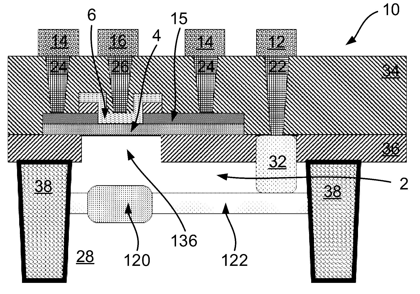
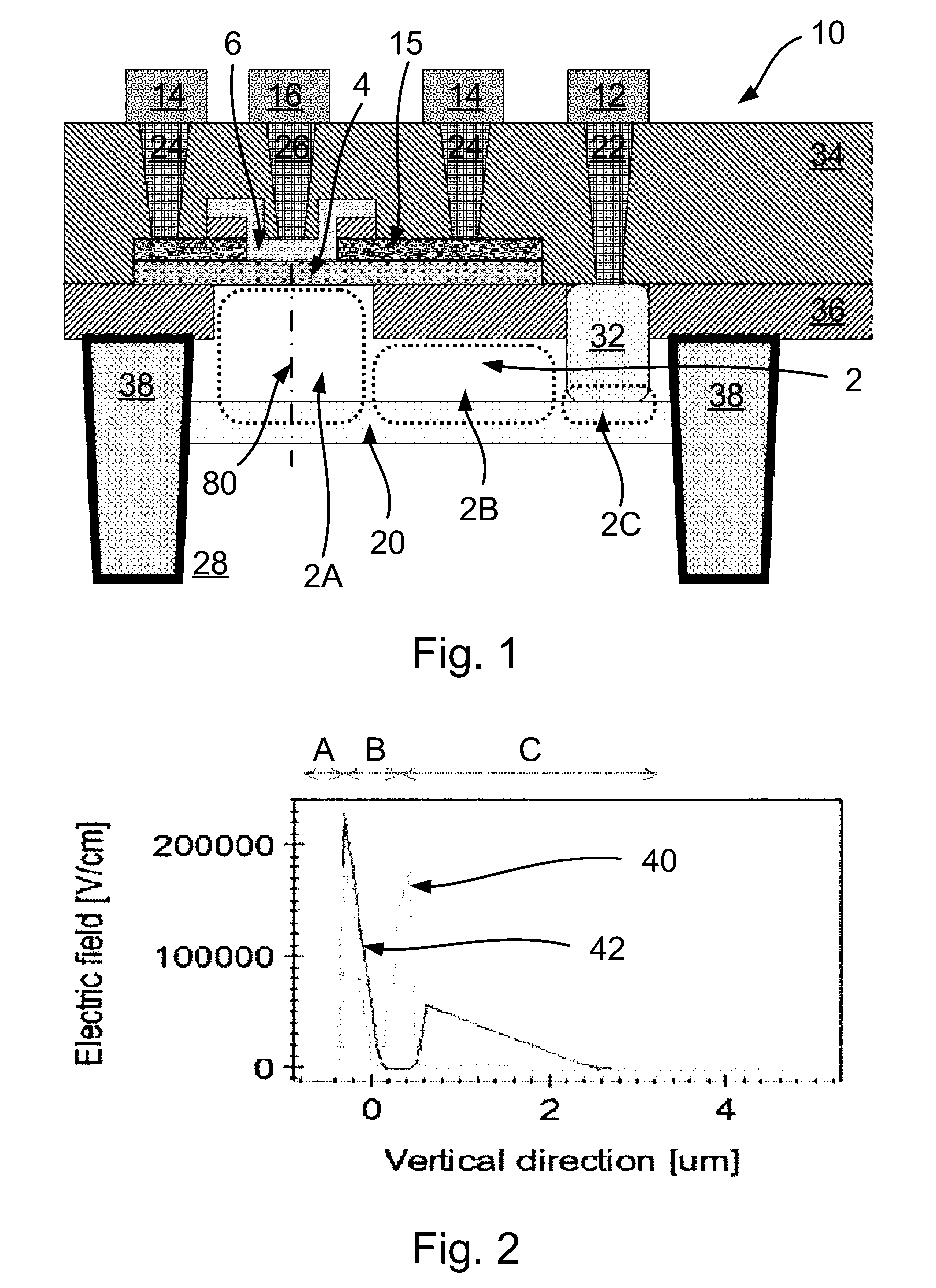
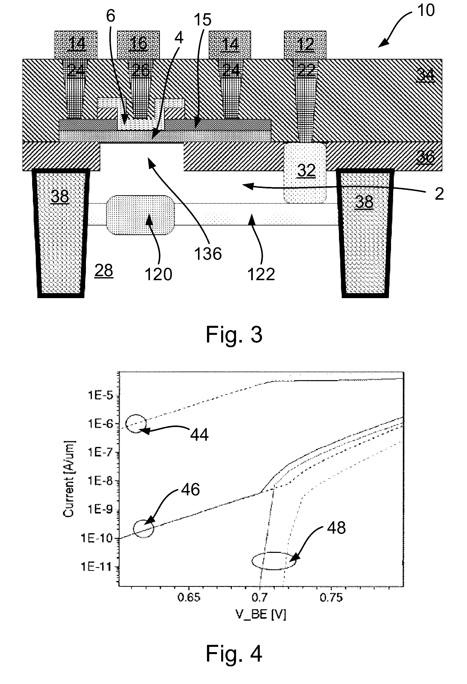
[0042]Embodiments of this invention can provide an improved semiconductor device comprising a bipolar transistor. The bipolar transistor may be a vertical device in the sense that the base and emitter may be located above the collector on a semiconductor substrate. The collector includes a laterally extending drift region. Typically, the collector-base junction may be located at or near a first end of the laterally extending region of the collector. In some examples, the collector may have two laterally extending drift regions each extending away from a centrally located collector base junction. In some embodiments, the device may be provided in the form of a ring in which the laterally extending drift region extends away from a centrally located collector base junction.

[0043]One or more contact(s) of the collector may be provided at a second end of the (or each) lat...


PUM


Abstract

A semiconductor device comprising a bipolar transistor and a method of making the same. A power amplifier including a bipolar transistor. The bipolar transistor includes a collector including a laterally extending drift region. The also includes a base located above the collector. The bipolar transistor further includes an emitter located above the base. The bipolar transistor also includes a doped region having a conductivity type that is different to that of the collector. The doped region extends laterally beneath the collector to form a junction at a region of contact between the doped region and the collector. The doped region has a non-uniform lateral doping profile. A doping level of the doped region is highest in a part of the doped region closest to a collector-base junction of the bipolar transistor.

Description

CROSS-REFERENCE TO RELATED APPLICATIONS[0001]This application claims the priority under 35 U.S.C. §119 of European patent application no. 14184549.5, filed on Sep. 12, 2014, the contents of which are incorporated by reference herein.FIELD OF THE INVENTION[0002]This invention relates to a bipolar transistor, a method of making a bipolar transistor and a power amplifier including a bipolar transistor.BACKGROUND OF THE INVENTION[0003]RF power amplifiers are key components in any high-frequency system and application. The demand for higher bandwidth and higher speeds for multimedia applications puts stringent requirements on these amplifiers such as high output power, linearity and efficiency. Amplifiers comprising bipolar transistors (such as heterojunction bipolar transistors (HBTs) are often used in preference to CMOS-based devices for RF power amplifiers because of their excellent performance at high frequencies.[0004]A limitation of silicon based devices (e.g. SiGe HBTs) is that th...

Claims


Application Information

Patent Timeline
Patent Type & Authority Patents(United States)
IPC IPC(8): H01L29/06H01L29/417H03F3/21H01L29/66H01L21/324H01L29/737H01L29/735H01L29/08H01L29/36
CPCH01L29/063H01L21/324H01L29/0649H01L29/0821H01L29/36H01L29/41708H01L29/6625H01L29/66242H01L29/735H01L29/7378H03F3/21H01L29/0684H01L29/7371
Inventor VANHOUCKE, TONYDINH, VIET THANHMAGNEE, PETRUS HUBERTUS CORNELISIVO, PONKYKLAASSEN, DIRKAL-SA'DI, MAHMOUD SHEHAB MOHAMMAD
Owner NXP BV
Why Eureka
Try Eureka