
Heat conductor device and method of forming a heat conductor device

a heat conductor and heat conductor technology, applied in the direction of cooling/ventilation/heating modifications, semiconductor/solid-state device details, and modifications by conduction heat transfer, can solve the problems of limiting radiation, limiting the size of a possible current loop, and reducing the effective electrical conductivity of the heat conductor device. , to achieve the effect of efficient formation

Active Publication Date: 2017-02-14
TOP VICTORY INVESTMENTS
View PDF7 Cites 2 Cited by
  • Summary
  • Abstract
  • Description
  • Claims
  • Application Information

AI Technical Summary

Benefits of technology

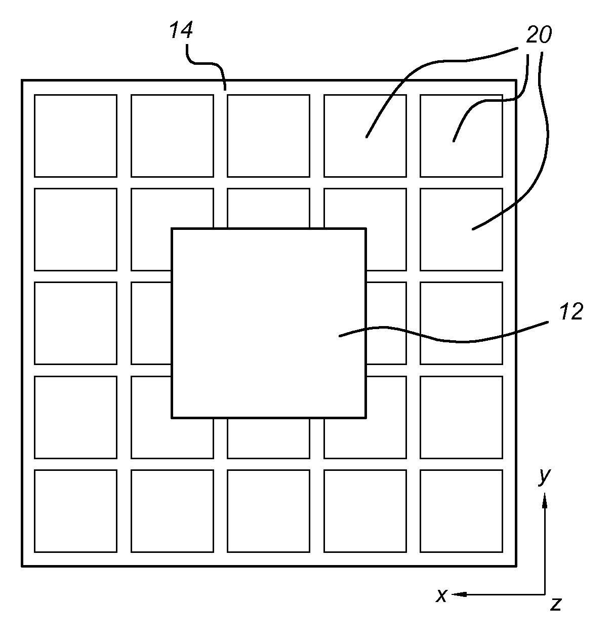
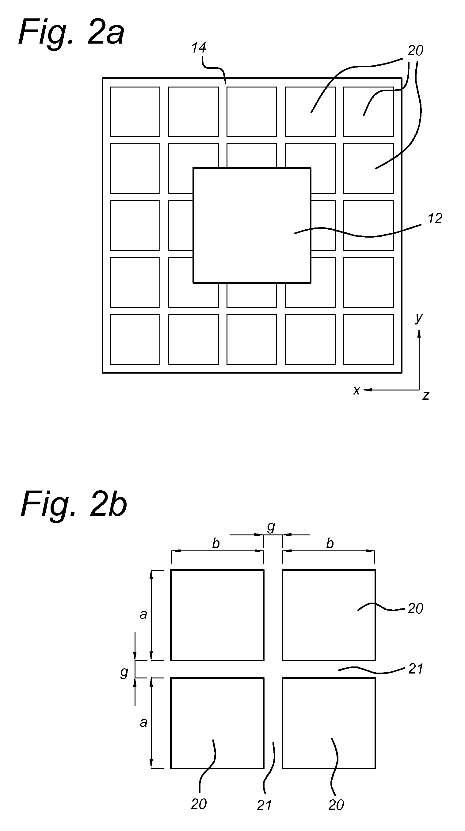
[0010]Each tile has an area that is small enough to prevent an individual tile from absorbing electromagnetic energy originating from the high-frequency currents inside the electrical component. At the same time, each tile has an area that is as large as possible in order to improve the heat conducting properties of the heat spreader layer and thus of the heat conductor device. Each gap forms a distance between adjacent tiles that is large enough to function as a barrier against electrical currents in the frequency range of the electrical component. At the same time, each gap is as small as possible to improve the heat conducting properties of the heat spreader layer and thus of the heat conductor device. As a result, the patterned heat spreader maximally increases the effective thermal conductivity of the heat conductor device, while minimally increasing the effective electrical conductivity of the heat conductor device.
[0029]In an embodiment according the invention, the pattern is provided through injection moulding the body around a substrate on which the pattern is formed. In this manner, the pattern can be efficiently formed inside a heat spreader device body.

Problems solved by technology

As a result, the patterned heat spreader maximally increases the effective thermal conductivity of the heat conductor device, while minimally increasing the effective electrical conductivity of the heat conductor device.
Furthermore, if the island size is well below the EM wavelength, the conducting islands will not function as an antenna, and the small size will also limit the size of a possible current loop, thereby limiting radiation as well.

Method used


Image

  • Heat conductor device and method of forming a heat conductor device
  • Heat conductor device and method of forming a heat conductor device
  • Heat conductor device and method of forming a heat conductor device

Examples


Embodiment Construction

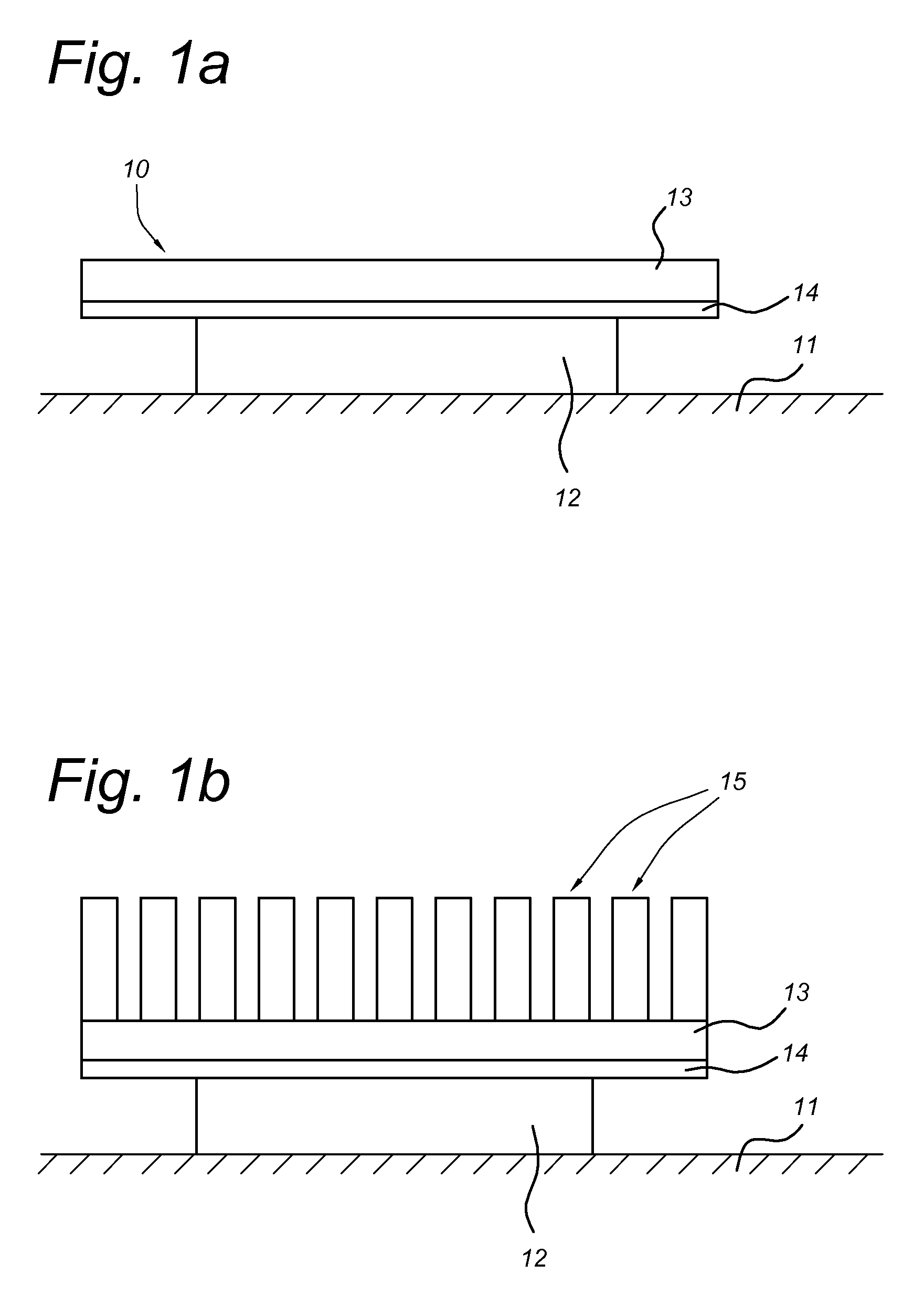
[0040]FIG. 1a schematically shows a heat conductor device 10 provided in thermal contact with an electrical component 12, in the present example an integrated circuit (IC) 12. The heat conductor device 10 comprises a body 13 made of plastic. Plastic advantageously has an essentially zero electrical conductivity, and thus does not give rise to the problems of radiating electromagnetic radiation if the plastic is provided on top of a high-frequency IC. Instead of plastic, any other material having a sufficiently low electrical conductivity can be used. A typical thickness of the body is between 0.5 and 5 mm, for example 1.5 mm. The body 13 is provided with a heat spreader 14 which will now be discussed in more detail in reference to FIGS. 2a and 2b. In the example of FIG. 1a, the heat spreader is located between the IC 12 and the body 13. In an alternative configuration, the heat spreader may be provided on top of the body 13, not facing the IC 12.

[0041]FIG. 1b shows a further alterna...


PUM


Abstract

The invention provides a heat conductor device (10) for removing heat from an electrical component (12) operating in a frequency range, the device comprising a body (13) having a first thermal conductivity, characterized in that the body (13) is provided with a heat spreader (14) comprising a pattern of thermally conducting tiles (20, 50, 51, 52, 61) separated by gaps (21), the tiles having a second thermal conductivity higher than the first thermal conductivity, wherein each tile has at most a maximum area value and the gaps have at least a minimum gap width, and the maximum area and the minimum width are dimensioned for conforming to a predetermined electromagnetic interference characteristic of the heat conductor device when combined with the electrical component operating in the frequency range. The invention also provides a method for forming a heat conductor device.

Description

FIELD OF THE INVENTION[0001]The invention relates to a heat conductor device for removing heat from an electrical component, particularly an electrical component that functions at a high frequency, for example in the GigaHertz (GHz) domain. The invention also relates to a method of forming a heat conductor device.BACKGROUND OF THE INVENTION[0002]An electrical component that needs cooling is placed in thermal contact with a thermally conductive material, also called a heat conductor device or heat sink. However, materials with good thermal conductivity (such as metal) also tend to have good electrical conductivity.[0003]A nearby layer with good electrical conductivity is problematic when used in conjunction with high frequency devices such as for processor integrated circuits (ICs) or memory ICs operating in the Megahertz (MHz) or Gigahertz (GHz) domain. In these applications, the conducting surface of the surrounding layer acts as a radiator for source currents which are present int...

Claims


Application Information

Patent Timeline
Patent Type & Authority Patents(United States)
IPC IPC(8): H05K7/20H01L23/367H01L23/373H01L23/66
CPCH05K7/2039H01L23/367H01L23/373H01L23/3731H01L23/3735H01L23/3736H01L23/3737H01L23/66H01L2924/0002H01L2924/00
Inventor LUITEN, GWENDOLYN ANITAPEETERS, LUC HENRI JOZEF
Owner TOP VICTORY INVESTMENTS
Learn More