
Switchable imaging device, switchable optical device, and display

a switchable optical device and switchable technology, applied in optics, instruments, electrical equipment, etc., can solve the problems of reducing the transmission rate by 65%, affecting the efficiency of light use, and affecting the transmission rate, so as to achieve high quality and reduce the transmission rate. , the effect of reducing the transmission ra

Active Publication Date: 2017-03-14
SHARP KK
View PDF28 Cites 4 Cited by
  • Summary
  • Abstract
  • Description
  • Claims
  • Application Information

AI Technical Summary

Benefits of technology

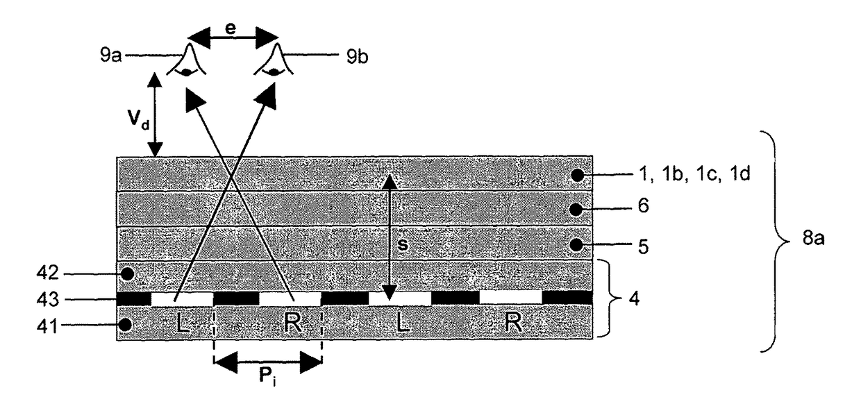
[0020]An aspect of the invention comprises a liquid crystal cell that forms a switchable imaging optical device. The switchable imaging optical device can be used in conjunction with an image display, for example, a liquid crystal display (LCD), organic light emitting diode (OLED) display etc. in order to yield a display system that has at least two modes of operation. In a first mode of operation (2D mode), the optical element does not perform an imaging function, thus enabling conventional, high quality 2D images to be viewed on the image display. In a second mode of operation (3D mode), the imaging optical element does perform an imaging function, enabling high quality autostereoscopic 3D images to be viewed on the image display. Switching between the 2D mode and the 3D mode is achieved via the application of an electric field to the liquid crystal layer. In the 3D mode, the optical element forms an array of GRIN lenses and an array of parallax barriers. The parallax barrier regions attenuate the transmission of light. The combination of GRIN lenses and parallax barriers image light from the pixels of the image display to the user's eyes. Consequently, the user is able to view high quality 3D images on the image display.
[0021]The switchable imaging optical device combines the positive features of the liquid crystal parallax barrier technology (low manufacturing costs, high image quality in the 2D mode and low 3D crosstalk in the 3D mode) with the positive features of a switchable lens system (high brightness in the 3D mode). Consequently, a superior switchable imaging optical device for the use in 3D and multi-view applications has been realised. The switchable imaging optical device has great design flexibility since the proportion of parallax barrier to GRIN lens ratio can be varied and customised for any given application.

Problems solved by technology

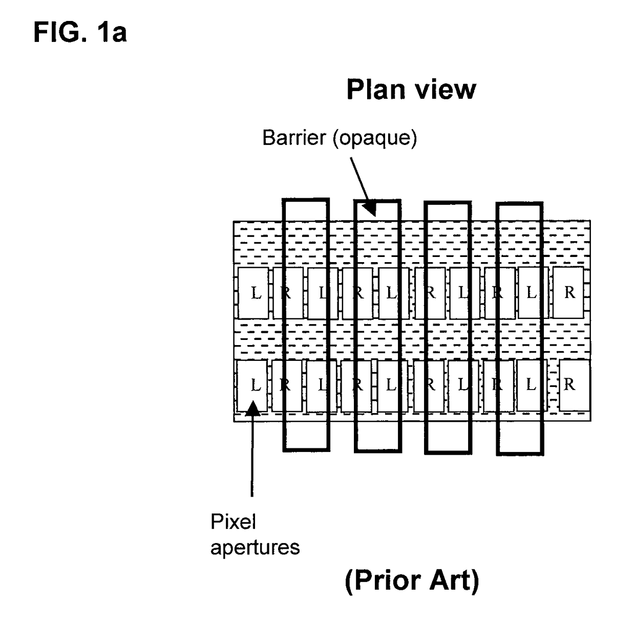
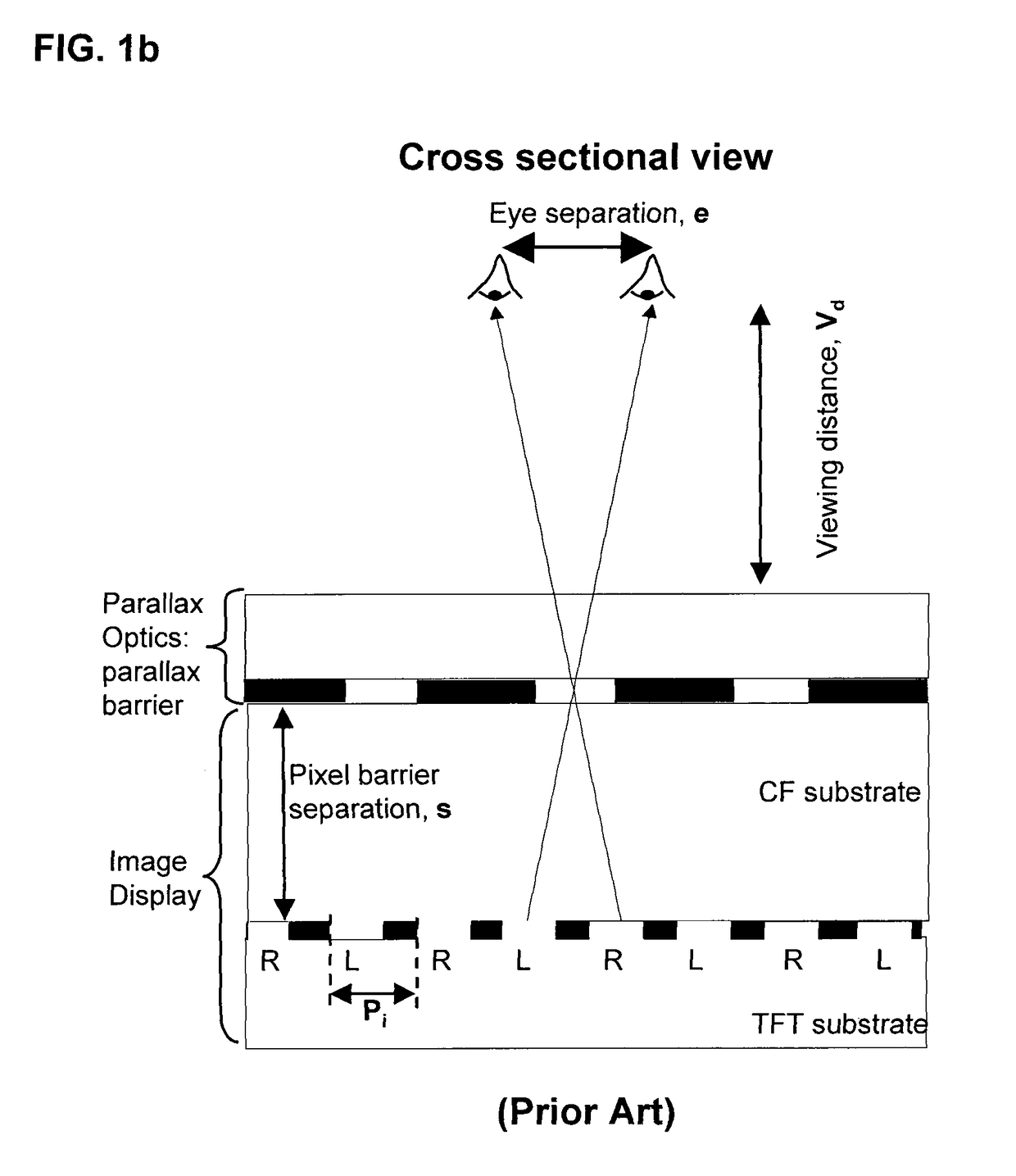
Using the technologies illustrated in FIGS. 1a to 2b would yield a 2D image with half the native resolution of the image display—this is highly undesirable.
However, switchable parallax barrier technology has the disadvantage that the parallax barrier absorbs light in the 3D mode, reducing transmission by ˜65%.
This inefficient light usage is a major disadvantage since the 2D mode and 3D mode will have a significantly different brightness.
Boosting the brightness of the 3D mode can be achieved at the expensive of increased power consumption, which is highly undesirable, especially for mobile products.
A first disadvantage of this technology is that the switchable lenses are more complicated and expensive to manufacture than a switchable parallax barrier.
A second disadvantage of this technology is the degradation of the 2D mode image quality.
This image degradation occurs because the refractive index of the liquid crystal varies as function of temperature and wavelength in a manner that does not exactly match that of the lens material.
Consequently, a residual lensing effect occurs that causes an observable brightness non-uniformity.
The disadvantage of this system is that the manufacture of electro-wetting lenses is complicated and expensive.
The LC lens technologies described above have the disadvantage that the 3D mode is not high quality because the metric of 3D crosstalk for LC lenses is inferior to that of switchable parallax barrier technologies.

Method used


Image

  • Switchable imaging device, switchable optical device, and display
  • Switchable imaging device, switchable optical device, and display
  • Switchable imaging device, switchable optical device, and display

Examples


Embodiment Construction

[0116]With reference to FIGS. 3a and 3b, FIGS. 4a and 4b and FIGS. 5a and 5b, a switchable imaging optical device 1 is fabricated that comprises a liquid crystal cell. With reference to FIG. 6 and FIG. 7 the switchable imaging optical device 1 is then combined with an image display 4 to yield a 2D-3D switchable display system.

[0117]With reference to FIGS. 3a and 3b, FIGS. 4a and 4b and FIGS. 5a and 5b, fabrication of the switchable imaging optical device 1 will now be described. The first substrate 111 (shown face up in FIG. 3a) and second substrate 121 (shown face up in FIG. 4a) are coated with transparent electrodes 112, 122 respectively, for example, indium tin oxide (ITO). The electrode layer 122 of the second substrate 121 is patterned in a pre-determined fashion, as illustrated by FIG. 4a. The dashed line 124 in FIG. 4a shows the approximate spatial extent of the pixelated area of the image display 4. For a 2-View 3D display system which has 1 pixel per image, the pitch 1222, ...


PUM


Abstract

A switchable imaging device (1) has a first mode of operation in which the device performs an imaging function and a second mode of operation different from the first mode, for example a non-imaging mode. In the first mode of operation the device comprises at least one first region that performs a lensing action and at least one second region that at least partially absorbs light passing through the or each second region. The switchable imaging device (1) may be disposed in path of light through an image display panel (4). This provides a display that may be operable in either a directional display mode such as an autostereoscopic 3D display mode or a 2-D display mode, by controlling the switchable imaging device to be in its first mode or its second mode.

Description

TECHNICAL FIELD[0001]This invention relates to switchable imaging optics for use in autostereoscopic (no glasses) 3D displays and other multi-view displays.BACKGROUND ART[0002]For many years people have been trying to create better autostereoscopic 3D displays, and this invention provides a further advance in this field. An autostereoscopic display is a display that gives stereoscopic depth without the user needing to wear glasses. This is accomplished by projecting a different image to each eye. An autostereoscopic 3D display (hereafter 3D display) can be realised by using parallax optic technology such as a parallax barrier or lenticular lenses.[0003]The design and operation of parallax barrier technology for viewing 3D images is well described in a paper from the University of Tokushima Japan (“Optimum parameters and viewing areas of stereoscopic full colour LED display using parallax barrier”, Hirotsugu Yamamoto et al., IEICE trans electron, vol E83-c no 10 Oct. 2000).[0004]FIGS...

Claims


Application Information

Patent Timeline
Patent Type & Authority Patents(United States)
IPC IPC(8): H04N13/04G02B27/22G02B27/26G02B3/00G02B30/25G02B30/31
CPCH04N13/0402G02B27/2214G02B27/26G02B3/0087H04N13/302G02B30/25G02B30/31H04N13/305H04N13/361G02B30/27
Inventor SMITH, NATHAN JAMESZAWADZKI, ALEXANDERBROUGHTON, BENJAMIN JOHNBAUM, ALEXANDRA
Owner SHARP KK
Learn More