Semiconductor device having buried gate structure and method for manufacturing the same, memory cell having the same and electronic device having the same

a technology of semiconductor devices and gate structures, applied in the field of semiconductor devices, can solve problems such as gidl exerting a substantial influence, and achieve the effect of improving refresh characteristics and improving performan

Active Publication Date: 2017-04-25
SK HYNIX INC
View PDF9 Cites 18 Cited by
  • Summary
  • Abstract
  • Description
  • Claims
  • Application Information

AI Technical Summary

Benefits of technology

[0008]Still another embodiment of the present invention is directed to a memory cell capable of improving refresh characteristics.
[0009]Yet another embodiment of the present invention is directed to an electronic device with improved performance.

Problems solved by technology

Moreover, gate induced drain leakage (GIDL) exerts a substantial influence on the performance of the buried gate type transistor.

Method used


Image

  • Semiconductor device having buried gate structure and method for manufacturing the same, memory cell having the same and electronic device having the same
  • Semiconductor device having buried gate structure and method for manufacturing the same, memory cell having the same and electronic device having the same
  • Semiconductor device having buried gate structure and method for manufacturing the same, memory cell having the same and electronic device having the same

Examples


first embodiment

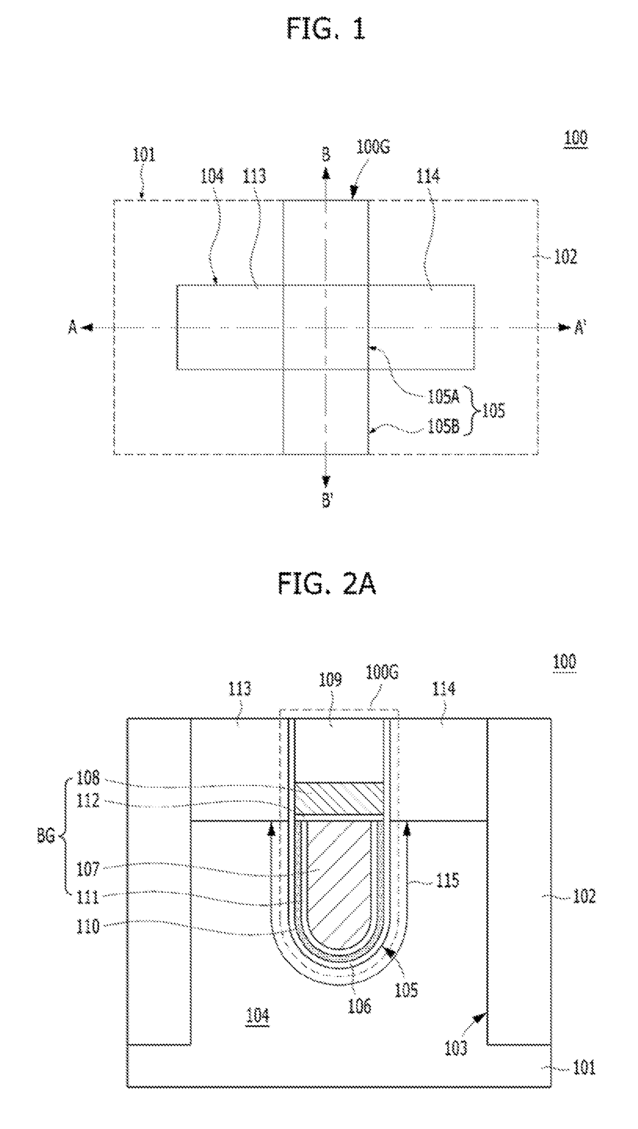
[0048]The semiconductor device 100 in accordance with the first embodiment will be described below in detail.

[0049]FIG. 2A and FIG. 2B are cross-sectional views of the semiconductor device in accordance with the first embodiment. FIG. 2A is a cross-sectional view taken along the line A-A′ of FIG. 1. FIG. 2B is a cross-sectional view taken along the line B-B′ of FIG. 1.

[0050]The semiconductor device 100 may be formed in the substrate 101. The substrate 101 may be a material suitable for semiconductor processing. The substrate 101 may include a semiconductor substrate. The substrate 101 may be formed of a silicon-containing material. The substrate 101 may include one or more of silicon, monocrystalline silicon, polysilicon, amorphous silicon, silicon germanium, monocrystalline silicon germanium, polycrystalline silicon germanium, carbon-doped silicon, a combination thereof, and a multi-layer thereof. The substrate 101 may include another semiconductor material such as germanium. Also,...

second embodiment

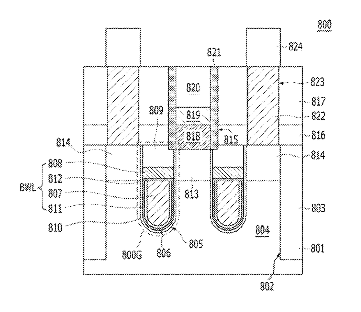
[0107]FIG. 6 is a cross-sectional view illustrating a semiconductor device in accordance with a Some components of a semiconductor device 200 except for a buried gate structure 200G may be the same as those of the semiconductor device 100.

[0108]The semiconductor device 200 may be formed in a substrate 201. A buried gate structure 200G of the semiconductor device 200 may be embedded in a gate trench 205. The buried gate structure 200G may be disposed in an active region 204 between a first impurity region 213 and a second impurity region 214, and extend in an isolation layer 202. The isolation layer 202 may be formed by filling an isolation trench 203 with a dielectric material.

[0109]The buried gate structure 200G may include a gate dielectric layer 206, a gate electrode BG, a work function adjusting liner 210H, a capping layer 209 and a work function liner 210L. The gate electrode BG may be positioned at a level lower than the top surface of the active region 204. The gate electrod...

third embodiment

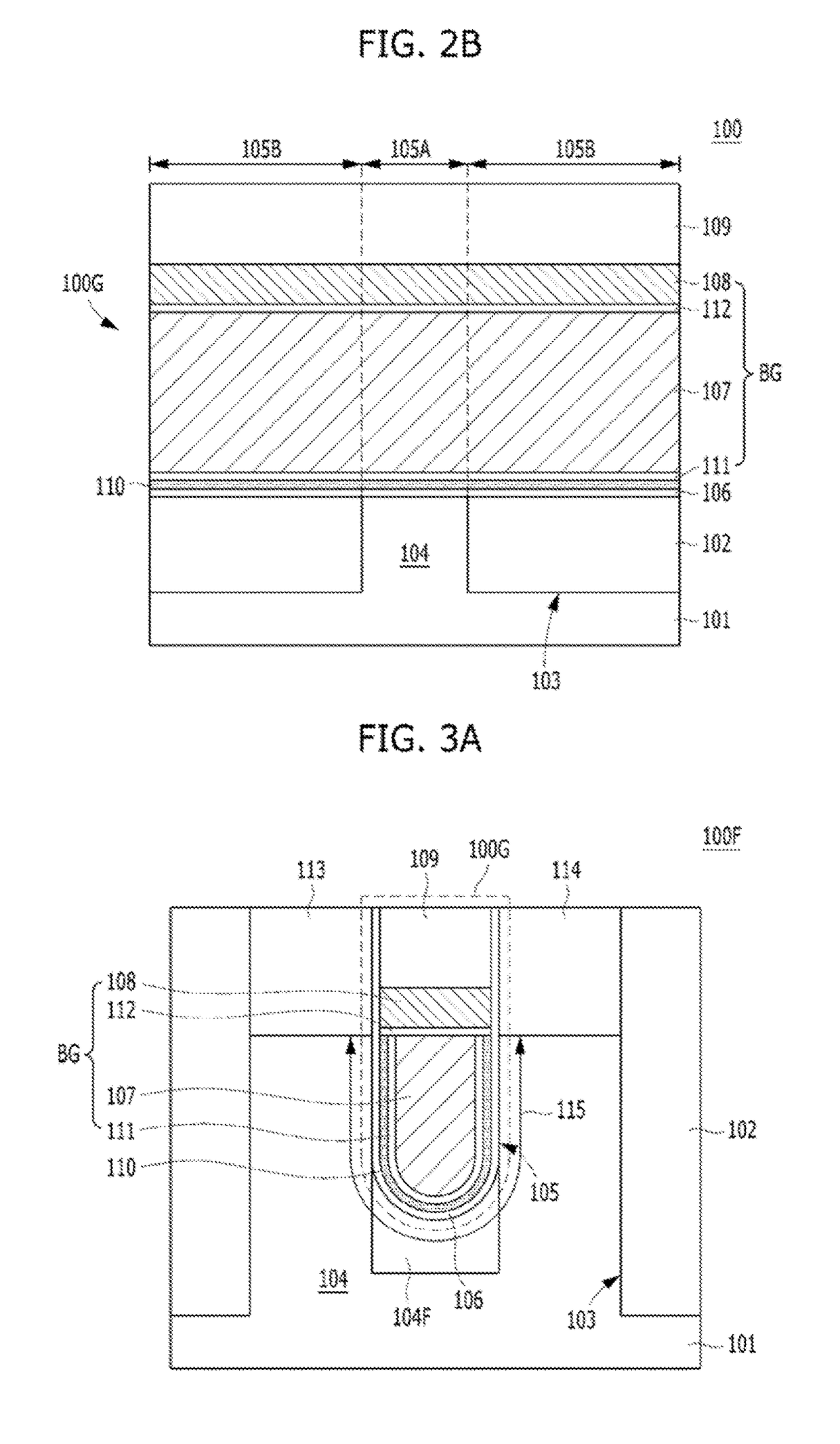
[0158] the work function adjusting liner 310H may be formed of a material which induces a high work function, and work function liner 310L may be formed of a material having a low work function.

[0159]By the work function adjusting liner 310H, a threshold voltage Vt may be adjusted. For example, the threshold voltage may be shifted by the work function adjusting liner 310H. A dipole may be formed at an interface between the work function adjusting liner 310H and the gate dielectric layer 306 by the work function adjusting liner 310H. The dipole may be used to increase the work function of the lower buried portion 307, and thus shift the threshold voltage. As a result, the channel dose may be decreased by the work function adjusting liner 310H.

[0160]Since the channel dose may be decreased by the work function adjusting liner 310H, the dose of the local channel doping may be decreased or the local channel doping may be omitted. As a result, in the embodiments, since a channel dose is d...


PUM


Abstract

A semiconductor device includes a substrate comprising a trench; a gate dielectric layer formed over a surface of the trench; a gate electrode positioned at a level lower than a top surface of the substrate, and comprising a lower buried portion embedded in a lower portion of the trench over the gate dielectric layer and an upper buried portion positioned over the lower buried portion; and a dielectric work function adjusting liner positioned between the lower buried portion and the gate dielectric layer; and a dipole formed between the dielectric work function adjusting liner and the gate dielectric layer.

Description

CROSS-REFERENCE TO RELATED APPLICATIONS[0001]The present application claims priority of Korean Patent Application No. 10-2015-0056595, filed on Apr. 22, 2015, which is incorporated herein by reference in its entirety.BACKGROUND[0002]1. Field[0003]Exemplary embodiments of the present invention relate to a semiconductor device, and more particularly, to a semiconductor device having a buried metal gate structure, a method for manufacturing the same, a memory cell having the same, and an electronic device having the same.[0004]2. Description of the Related Art[0005]A metal gate electrode is used to improve transistor performance. In particular, in a buried gate type transistor, adjusting the threshold voltage is required to carry out high performance operations. Moreover, gate induced drain leakage (GIDL) exerts a substantial influence on the performance of the buried gate type transistor.SUMMARY[0006]An embodiment of the present invention is directed to a buried gate structure capable...

Claims


Application Information

Patent Timeline
Patent Type & Authority Patents(United States)
IPC IPC(8): H01L29/78H01L29/51H01L29/423H01L27/108H01L29/66H01L29/49
CPCH01L27/10823H01L27/10876H01L29/4236H01L29/4958H01L29/4966H01L27/10814H01L29/513H01L29/517H01L29/66621H01L21/28H01L29/66477H01L29/78H01L29/785H10B12/315H10B12/34H10B12/053H10B12/488H01L21/02164H01L21/02175H01L21/02178H01L21/02181H01L21/02186H01L21/02189H01L29/511H01L21/823418H01L29/41783H01L29/66628
Inventor KANG, DONG-KYUNCHO, HO-JIN
Owner SK HYNIX INC
Why Eureka
Try Eureka