
Method for smoothing surface of a substrate containing gallium and nitrogen

Active Publication Date: 2017-05-09
KORRUS INC
View PDF264 Cites 2 Cited by
  • Summary
  • Abstract
  • Description
  • Claims
  • Application Information

AI Technical Summary

Benefits of technology

The invention provides a process that smooths the surface of a substrate and reduces damage and defects, making it better suited for making various devices like LED chips and power electronics.

Problems solved by technology

Unfortunately, conventional techniques have been inadequate.

Method used


Image

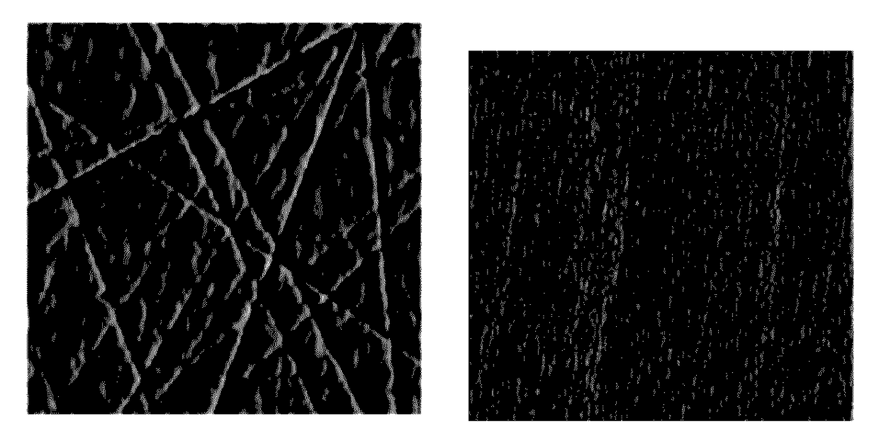
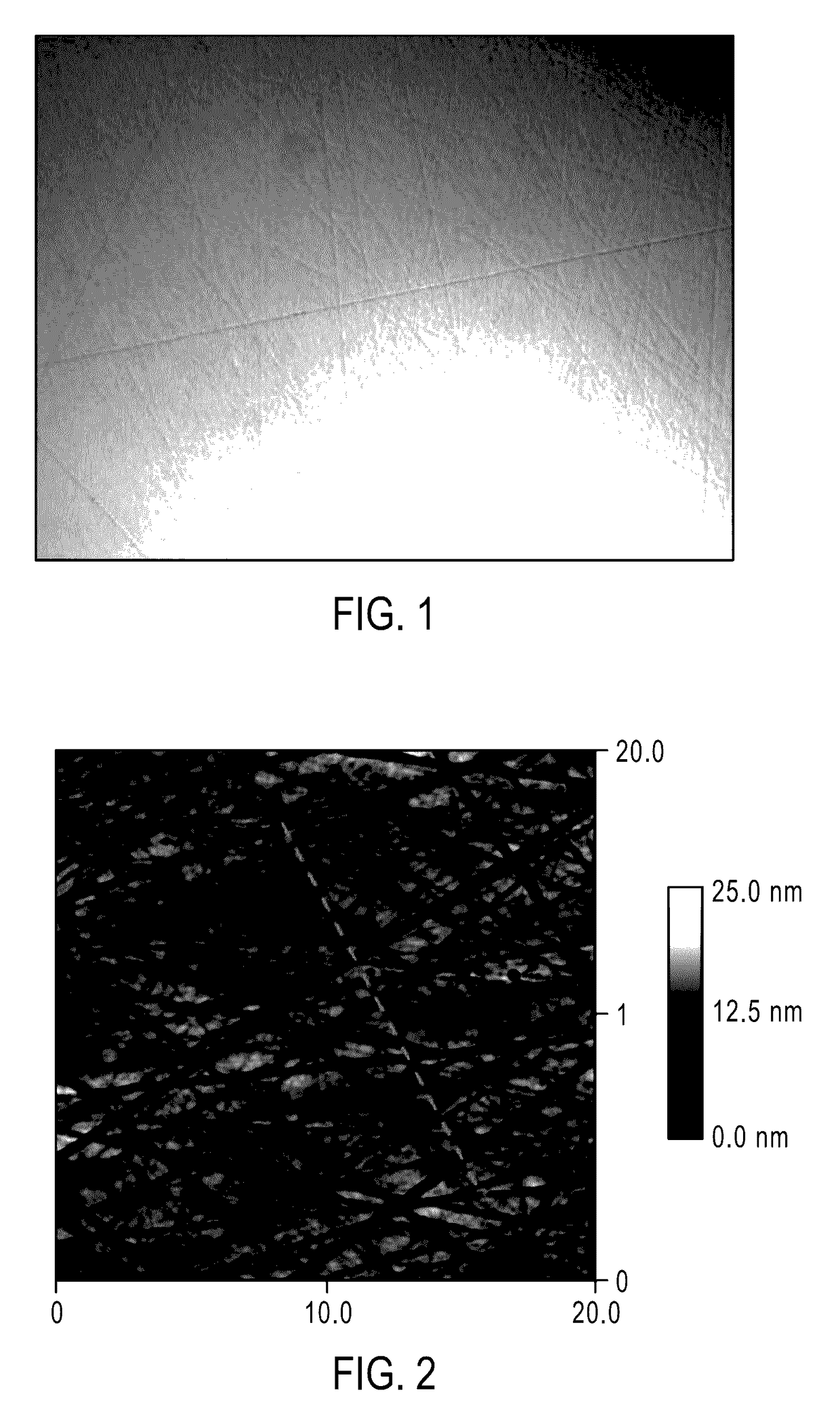
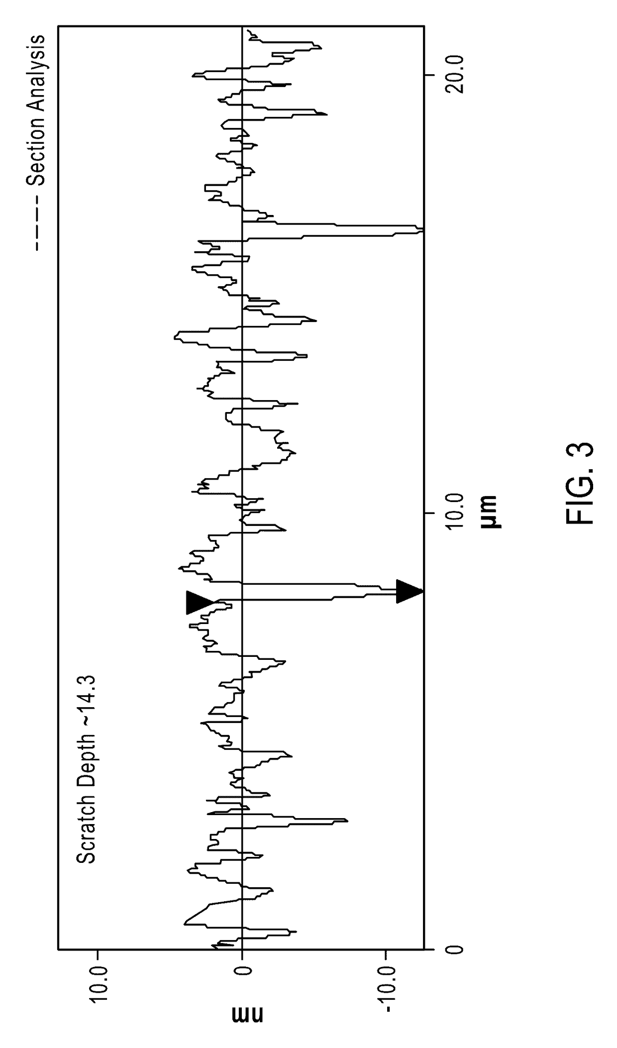
  • Method for smoothing surface of a substrate containing gallium and nitrogen
  • Method for smoothing surface of a substrate containing gallium and nitrogen
  • Method for smoothing surface of a substrate containing gallium and nitrogen

Examples


Embodiment Construction

[0022]As mentioned above, GaN substrates with a smooth surface are desirable. Often, achieving a smooth surface prior to the growth of an active region is a requirement for achieving high performance devices, such as LEDs and laser diodes. A smooth growth surface can provide many benefits, such as:

[0023]1. Sharp interfaces between layers;

[0024]2. Minimize roughness-induced scattering, thereby resulting in higher carrier mobility;

[0025]3. Reduced point defect densities;

[0026]4. Uniform alloy, dopant composition indium incorporation across wafer; and / or

[0027]5. Prevents 3-D growth mode.

[0028]Achieving a smooth surface morphology is often difficult, especially for bulk GaN substrates. An in-situ surface treatment is often required to generate the step-structure, required for 2-D step-flow growth mode. The surface treatment is usually carried out in-situ and consists of ramping the temperature in a growth chamber in ammonia and hydrogen ambient, followed by nitridation of the GaN surfac...


PUM


Abstract

Disclosed is a method for processing GaN based substrate material for manufacturing light-emitting diodes, lasers, and other types of devices. In various embodiments, a GaN substrate is exposed to nitrogen and hydrogen at a high temperature. This process causes the surface of the GaN substrate to anneal and become smooth. Then other processes, such as growing epitaxial layers over the surface of GaN substrate, can be performed over the smooth surface of the GaN substrate.

Description

[0001]This application claims the benefit of U.S. Provisional Application No. 61 / 526,355, filed on Aug. 23, 2011, which is incorporated by reference in its entirety.BACKGROUND OF THE INVENTION[0002]The invention is directed to optical devices. With the advent of semiconductor devices and applications thereof, GaN materials are being used for fabricating light emitting diodes (LEDs), lasers, and other types of devices. Typically, LEDs are formed over sapphire, silicon carbide, and on gallium nitride (GaN) substrates.[0003]To form devices (e.g., LED or laser devices) over a GaN substrate, it is desirable to have a smooth surface. In the past, various processing techniques have been developed to achieve this goal. Unfortunately, conventional techniques have been inadequate.SUMMARY OF THE INVENTION[0004]Embodiments provided by the present disclosure are directed to optical devices. More specifically, embodiments of the invention provide a method for processing GaN based substrate materi...

Claims


Application Information

Patent Timeline
IPC IPC(8): H01L33/32H01L21/02H01L33/00
CPCH01L21/0254H01L33/0075H01L21/02389H01L21/02658
Inventor CHAKRABORTY, ARPANTYAGI, ANURAG
Owner KORRUS INC
Learn More