Device isolation structure and manufacture method

a technology of isolation structure and manufacturing method, applied in the field of semiconductor devices, can solve the problems of large die size of integrated circuits and limit on device spacing, and achieve the effects of small dimension, good isolation, and simple manufacturing steps

Active Publication Date: 2017-05-16
SEMICON MFG INT (SHANGHAI) CORP
View PDF3 Cites 3 Cited by
  • Summary
  • Abstract
  • Description
  • Claims
  • Application Information

AI Technical Summary

Benefits of technology

[0006]Embodiments of the present invention provide an isolation pocket structure and method of fabrication. In an embodiment, a dielectric layer is disposed in the deep trench lined with heavily doped polysilicon. The dielectric material in deep trenches avoids breakdown or punch-through between devices and the doped polysilicon. The doped poly can be used as electrical pickup for applying a potential to the buried layer for junction isolation between the buried layer and substrate in the vertical direction. The dielectric layer and the anti-type dopant below the dielectric layer could offer additional isolation between two pockets at lateral direction. The fabrication steps are simple and create good isolation in a relatively small dimension. The lateral direction isolation is provided by the dielectric layer instead of junctions, which can reduce the dimension, enhance the noise immunity, and reduce cross-talks and latch-up.
[0023]As described above, the fabrication steps are simple and provide effective isolation in relatively small dimensions. The dielectric material can avoid breakdown or punch-through between devices and the buried pick-up doped poly. The doped poly picks up the buried layer and force potential onto the buried layer which will offer junction isolation between the buried layer and substrate at vertical direction. Before the dielectric layer deposition, anti-type dopant is implanted at the bottom of the trench. The anti-type dopant and the dielectric layer could offer the isolation between two pockets in the lateral direction. As a result, the lateral direction isolation is blocked by the dielectric layer instead of the junction, which will reduce the device dimension. Devices can be disposed into the isolation pocket structure, which could enhance noise immunity and reduce cross-talks and latch up.

Problems solved by technology

However, the inventors have observed that subsequent thermal processing can cause diffusion in the buried layer and out-diffusion from the doped polysilicon in the isolation pocket.
These diffusion regions can impose a limit on device spacing and lead to larger die size of the integrated circuit.

Method used


Image

  • Device isolation structure and manufacture method
  • Device isolation structure and manufacture method
  • Device isolation structure and manufacture method

Examples


Embodiment Construction

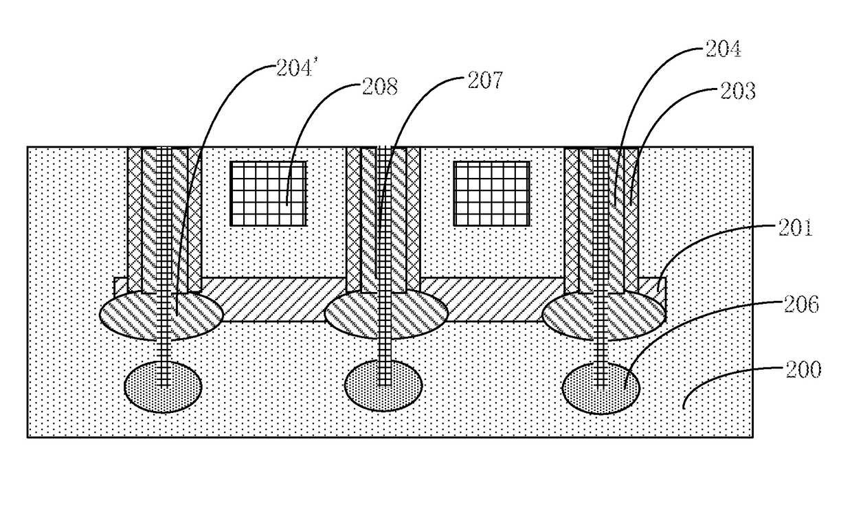
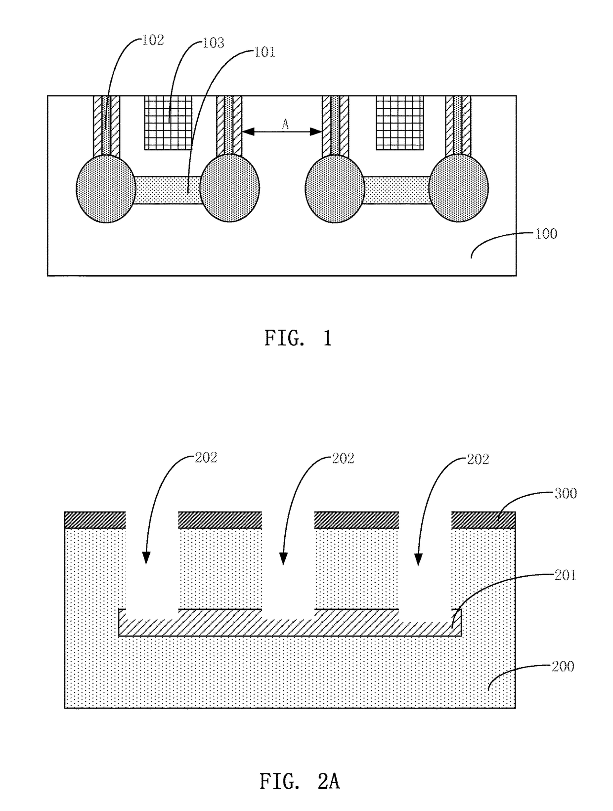
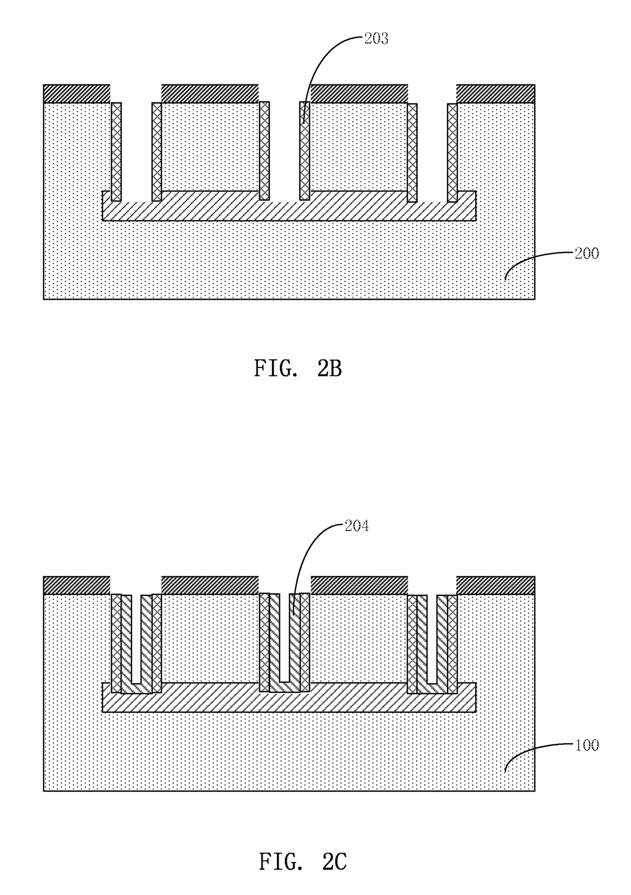
[0029]Embodiments of the present invention provide an isolation structure, its manufacturing method, and related electronic devices.

[0030]In the following description, numerous specific details are provided for a thorough understanding of the present invention. However, it should be appreciated by those of skill in the art that the present invention may be realized without one or more of these details. In other examples, features and techniques known in the art will not be described for purposes of brevity.

[0031]It should be understood that the drawings are not drawn to scale, and similar reference numbers are used for representing similar elements. Embodiments of the invention are described herein with reference to cross-section illustrations that are schematic illustrations of idealized embodiments (and intermediate structures) of the invention. The thickness of layers and regions in the drawings may be exaggerated relative to each other for clarity. Additionally, variations in th...


PUM


Abstract

A method for forming a semiconductor device includes forming a buried doped layer in a semiconductor substrate and forming a plurality of first trenches that expose the buried doped layer. A first dielectric layer is formed covering sidewalls of the first trenches, and a doped polysilicon layer is formed covering side surfaces of the first dielectric layer and bottom portions of the first trenches. The method also includes forming a second trench in each of the plurality of first trenches, each second trench extending through a bottom portion of the doped polysilicon layer and the buried doped layer into a lower portion of the substrate. The method also includes forming a second dielectric layer inside each second trench. An isolation pocket structure is formed that includes the doped buried layer at the bottom and sidewalls that includes the doped polysilicon layer sandwiched between the first and second dielectric layers.

Description

CROSS-REFERENCES TO RELATED APPLICATIONS[0001]This application claims priority to Chinese patent application No. 201410548682.X, filed on Oct. 16, 2014, the content of which is incorporated herein by reference in its entirety.BACKGROUND OF THE INVENTION[0002]The present invention relates to the field of semiconductor technology. Specifically, embodiments of the invention relate to semiconductor device isolation structures and manufacturing methods.[0003]In analog integrated circuits (IC), in order to obtain good noise immunity, a junction isolation pocket with a buried implant layer can be formed within the substrate. FIG. 1 is a cross-sectional diagram illustrating a conventional semiconductor device in a semiconductor substrate 100. As shown in FIG. 1, a device 103 is disposed in an isolation pocket having a doped polysilicon 102 in a deep trench structure at the side of a buried layer 101.[0004]However, the inventors have observed that subsequent thermal processing can cause diff...

Claims


Application Information

Patent Timeline
Patent Type & Authority Patents(United States)
IPC IPC(8): H01L29/06H01L21/762
CPCH01L21/76237H01L21/76286H01L21/763H01L21/765H01L23/552
Inventor YANG, GUANGLIPU, XIANYONGLIU, LITAI, CHIHCHUNGWANG, GANGNINGSUN, HONG
Owner SEMICON MFG INT (SHANGHAI) CORP
Why Eureka
Try Eureka