Supercharge Your Innovation With Domain-Expert AI Agents!

GOA circuit of reducing power consumption

a technology of power consumption and goa circuit, which is applied in the field of display technology, can solve the problems of increasing power consumption, increasing the high-low voltage difference of the clock signal ck(m), and higher power consumption of the goa circuit, so as to reduce the parasitic capacitance reduce the voltage level of the clock signal, and ease the loading of the clock signal

Active Publication Date: 2017-05-23
SHENZHEN CHINA STAR OPTOELECTRONICS TECH CO LTD
View PDF3 Cites 3 Cited by
  • Summary
  • Abstract
  • Description
  • Claims
  • Application Information

AI Technical Summary

Benefits of technology

The present invention provides a GOA circuit that reduces power consumption by controlling the (in)voltage levels of the clock signal and easing the signal's loading. This circuit also prevents abnormal sequence of scan driving signals and ensures normal function of the GOA circuit. The circuit includes a stage transfer signal for transmitting and backward feedback, while a pull-down holding module prevents electrical leakage. Overall, this circuit improves the reliability and stability of the GOA circuit.

Problems solved by technology

However, the GOA circuit according to prior art has drawbacks of increasing power consumption in comparison with the externally connected IC.
Under such circumstance, it results in larger high-low voltage difference of the clock signal CK(m), and the power consumption of the GOA circuit is higher.
However, if the high voltage of the clock signal CK(m) is not raised, then the propulsive force of the scan driving signal G(N) will be insufficient, which can easily cause the abnormal sequence of the scan driving signal G(N).

Method used


Image

  • GOA circuit of reducing power consumption
  • GOA circuit of reducing power consumption
  • GOA circuit of reducing power consumption

Examples


Embodiment Construction

[0066]For better explaining the technical solution and the effect of the present invention, the present invention will be further described in detail with the accompanying drawings and the specific embodiments.

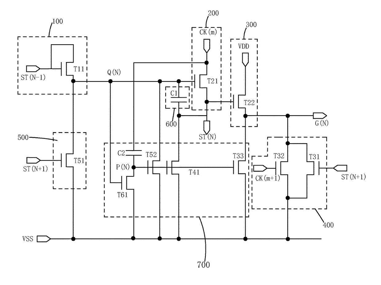
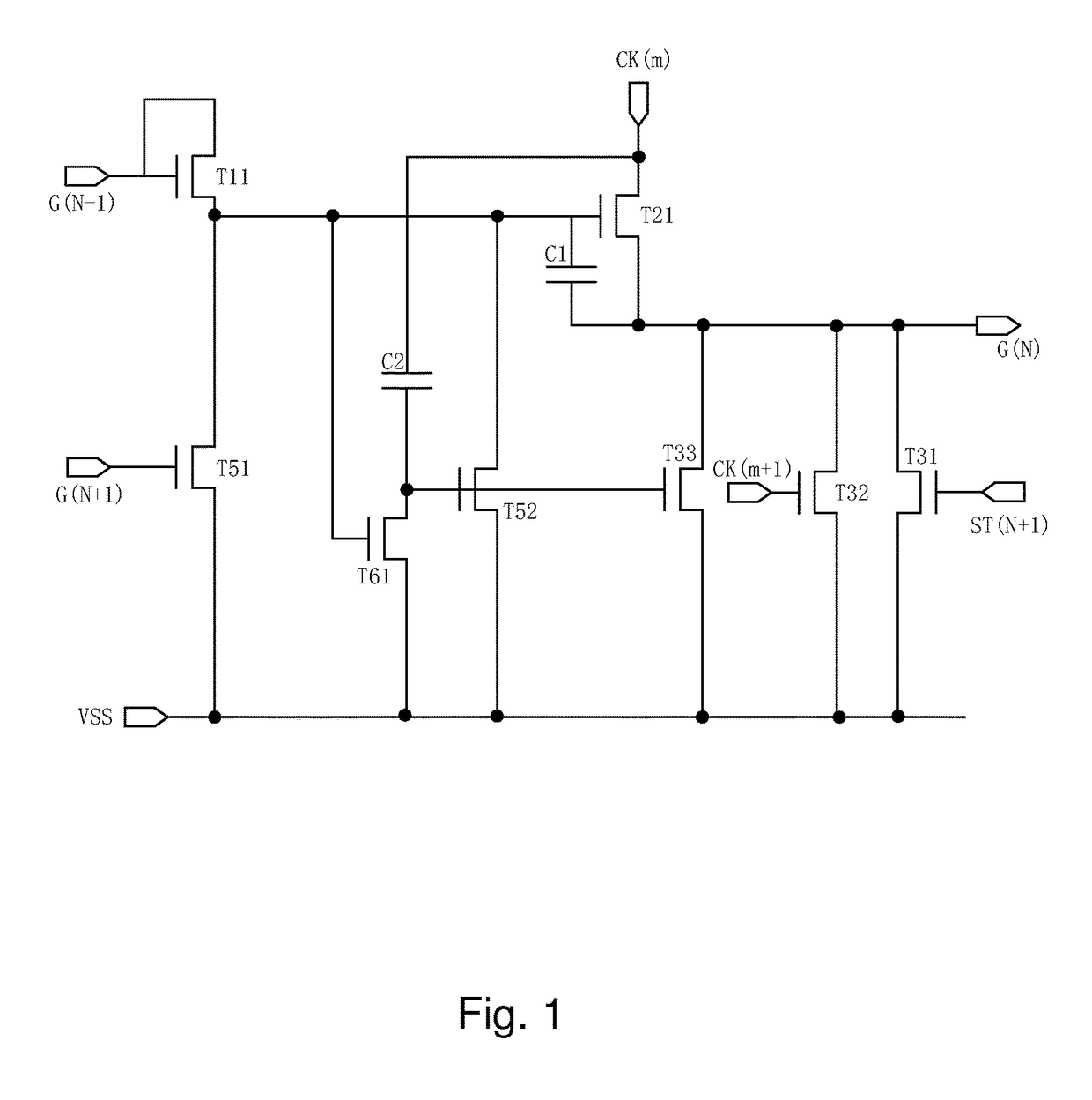
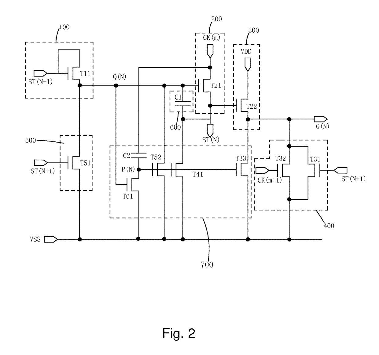
[0067]Please refer to FIG. 2. The present invention provides a GOA circuit of reducing power consumption, comprising a plurality of GOA unit circuits which are cascade connected, and the GOA unit circuit of every stage comprises a first pull-up controlling module 100, a second pull-up controlling and transmission module 200, a pull-up module 300, a first pull-down module 400, a second pull-down module 500, a bootstrap capacitor module 600 and a pull-down holding module 700, and each module comprises one or more thin film transistors.

[0068]N is set to be a positive integer and except the GOA unit circuit of the first stage and the GOA unit circuit of the last stage, in the GOA unit circuit of the Nth stage:

[0069]the first pull-up controlling module 100 comprises an eleventh thi...


PUM


Abstract

The present invention provides a GOA circuit of reducing power consumption. In the GOA unit circuit of the Nth stage, the twenty-second thin film transistor (T22) of the pull-up module (300) is controlled by the twenty-first thin film transistor (T21) of the second pull-up controlling and transmission module (200) to output the constant high voltage level (VDD) to the scan driving signal (G(N)) for reducing the parasitic capacitance of the clock signal, lowering the voltage level of the clock signal, easing the loading of the clock signal, and thus, to reduce the power consumption of the GOA circuit; the clock signal (CK(m)) is outputted to the stage transfer signal (ST(N)) through the twenty-first thin film transistor (T21), and the stage transfer signal (ST(N)) is employed for the transmission of the signal and the backward feedback to reduce the loading of the scan driving signal, and enhance the propulsive force of the scan driving signal, and the normal function of the GOA circuit can be ensured; and the forty-first thin film transistor (T41) is added in the pull-down holding module (700) to pull down the stage transfer signal (ST(N)) for preventing the electrical leakage of the twenty-second thin film transistor (T22).

Description

FIELD OF THE INVENTION[0001]The present invention relates to a display technology field, and more particularly to a GOA circuit of reducing power consumption.BACKGROUND OF THE INVENTION[0002]The Liquid Crystal Display (LCD) possesses advantages of thin body, power saving and no radiation to be widely used in many application scope, such as LCD TV, mobile phone, personal digital assistant (PDA), digital camera, notebook, laptop, and dominates the flat panel display field.[0003]Most of the liquid crystal displays on the present market are backlight type liquid crystal displays, which comprise a liquid crystal display panel and a backlight module. The working principle of the liquid crystal display panel is that the Liquid Crystal is injected between the Thin Film Transistor Array Substrate (TFT array substrate) and the Color Filter (CF). The light of backlight module is refracted to generate images by applying driving voltages to the two substrates for controlling the rotations of the...

Claims


Application Information

Patent Timeline
IPC IPC(8): G09G3/3266G09G3/36
CPCG09G3/3648G09G3/3674G09G2310/08G09G2330/023G09G2300/0809G09G3/3677G09G2300/0408G09G2310/0286G09G2330/021
Inventor MEI, WENLIN
Owner SHENZHEN CHINA STAR OPTOELECTRONICS TECH CO LTD
Features
  • R&D
  • Intellectual Property
  • Life Sciences
  • Materials
  • Tech Scout
  • Unparalleled Data Quality
  • Higher Quality Content
  • 60% Fewer Hallucinations
Learn More