Tape carrier package, method of manufacturing the same and chip package

a technology of tape carrier and chip, which is applied in the direction of printed circuit aspects, printed circuit non-printed electric components association, semiconductor/solid-state device details, etc. it can solve the problems of increasing production cost and time of tape carrier packages, generating equipment load, and reducing the production cost of tape carrier packages. , to achieve the effect of excellent reliability and durability, saving drying time, and reducing production costs

Active Publication Date: 2017-06-06
LG INNOTEK CO LTD
View PDF33 Cites 0 Cited by
  • Summary
  • Abstract
  • Description
  • Claims
  • Application Information

AI Technical Summary

Benefits of technology

[0013]According to some embodiments of the present invention, a tape carrier package, a method of manufacturing the same, and a chip package are advantageous in that the punching process, and the processes of laminating and drying the copper layer which are necessary for the conventional method of manufacturing the tape carrier package can be omitted, and accordingly, a production cost of the tape carrier package can be reduced and the time required for the drying process can be saved.
[0014]Also, according to some embodiments of the present invention, since a surface roughness is formed on the adhesive layer of the base element, adhesive strength with the molding portion is improved, thereby enabling a chip package with excellent reliability and durability to be provided.

Problems solved by technology

Thus, when developing a product, due to CNC punching, the delay in development and equipment load are generated.
Furthermore, it is to be costly to apply the adhesive in a semi-hardened state to the insulating layer 10.
Thus, this became a factor that increases the production cost and time of the tape carrier package.

Method used


Image

  • Tape carrier package, method of manufacturing the same and chip package
  • Tape carrier package, method of manufacturing the same and chip package
  • Tape carrier package, method of manufacturing the same and chip package

Examples


Embodiment Construction

[0019]Hereinafter, preferred embodiments of the present invention will be described in detail with reference to the accompanying drawings. In the following description, it is to be noted that, when the functions of conventional elements and the detailed description of elements related with the present invention may make the gist of the present invention unclear, a detailed description of those elements will be omitted.

[0020]Furthermore, it should be understood that the shape and size of the elements shown in the drawings may be exaggeratedly drawn to provide an easily understood description of the structure of the present invention rather than reflecting the actual sizes of the corresponding elements.

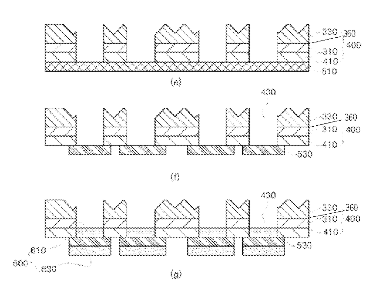
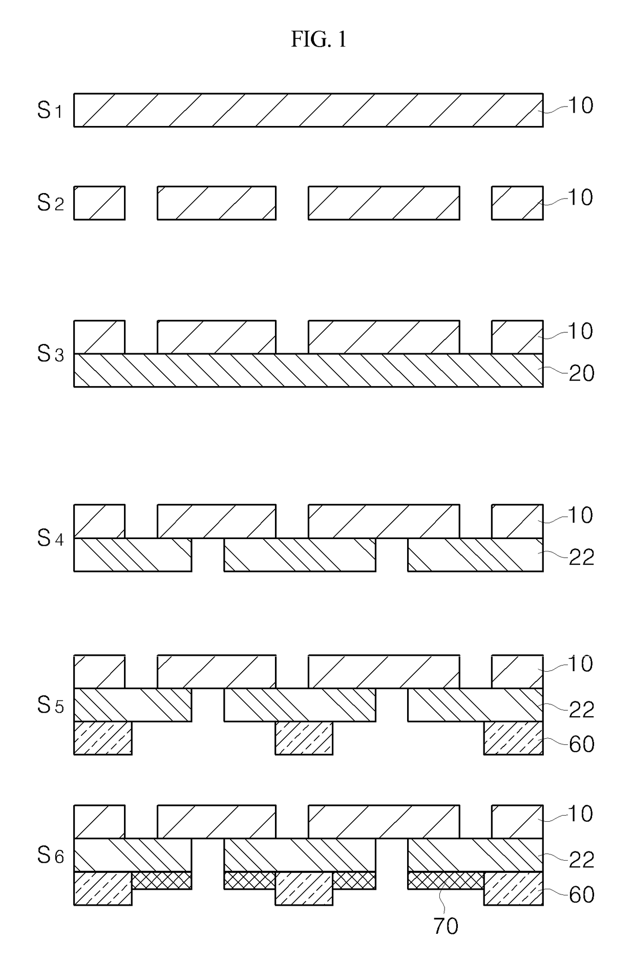
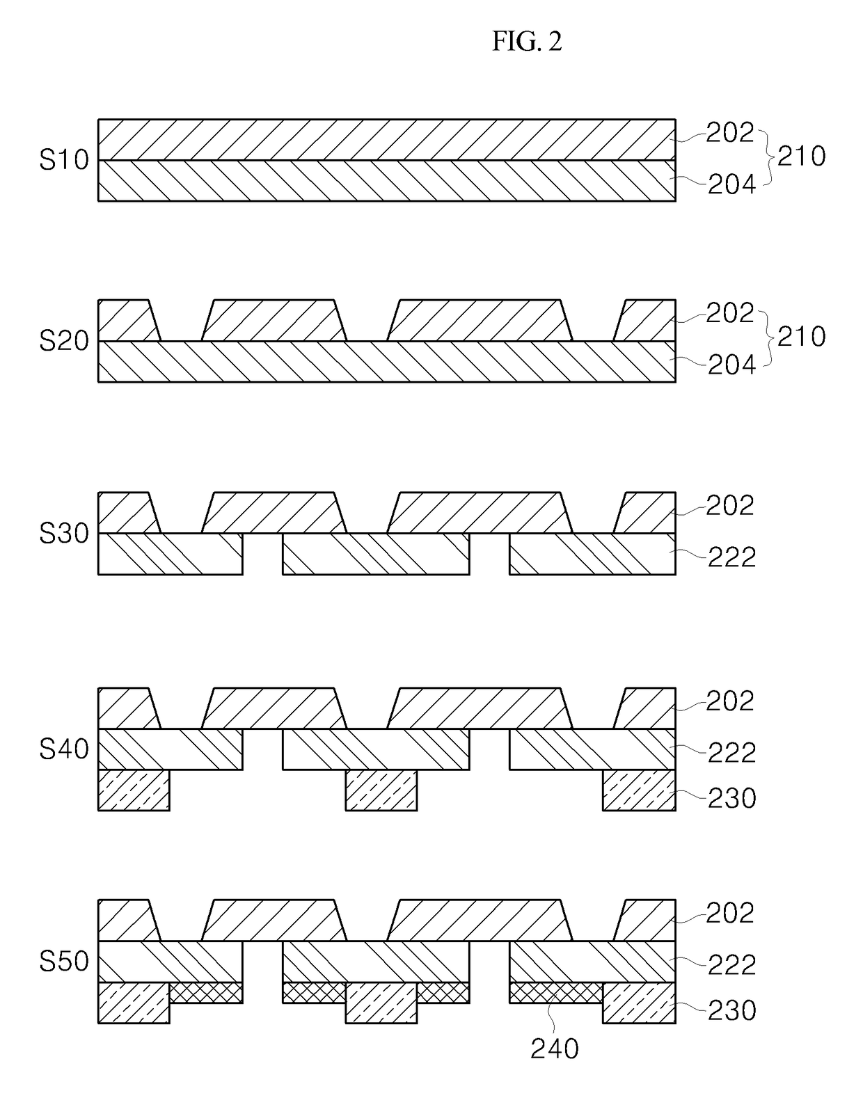
[0021]FIG. 2 is a view showing a process of manufacturing a tape carrier package according to a preferred exemplary embodiment of the present invention.

[0022]Referring to FIG. 2, a flexible copper clad laminate (hereinafter referred to as the “FCCL”) film 210 is prepared (S10). The FCCL...


PUM


Abstract

Provided are a tape carrier package and a method of manufacturing the same, the method, including: forming through holes by performing a drill process using a laser to an insulating film of a flexible copper clad laminate (FCCL) film consisting of the insulating film and a copper layer; forming a circuit pattern layer by performing an etching process to the copper layer of the FCCL film; and selectively forming a plating layer on the circuit pattern layer. The method of manufacturing the tape carrier package according to the present invention is advantageous because a punching process, and processes for laminating and drying the copper layer which are necessary for the conventional method of manufacturing the tape carrier package can be omitted, a production cost of the tape carrier package is reduced, and the time required for the drying process is saved.

Description

CROSS-REFERENCE TO RELATED APPLICATIONS[0001]This application is the U.S. national stage application of International Patent Application No. PCT / KR2012 / 009284, filed Nov. 6, 2012, which claims priority to Korean Application Nos. 10-2011-0116289, filed Nov. 9, 2011, and 10-2011-0125656, filed Nov. 29, 2011, the disclosures of each of which are incorporated herein by reference in their entirety.TECHNICAL FIELD[0002]Embodiments of the present invention relate to a tape carrier package, a method of manufacturing the same and a chip package.BACKGROUND ART[0003]A tape carrier package (TCP) is a semiconductor package manufactured by bonding an Au bump of an LCD driver IC (LDI) and an inner lead of a carrier tape with a thereto compression bonding method using a tape automated bonding (TAB) technology and applying resin thereto.[0004]The carrier tape is configured such that a copper foil is bonded to a polyimide film using an adhesive, a circuit is formed in the copper foil through a proces...

Claims


Application Information

Patent Timeline
Patent Type & Authority Patents(United States)
IPC IPC(8): H05K3/46H01L21/48H05K1/11H05K3/00H05K1/18H01L23/498H05K1/03
CPCH05K1/115H01L21/486H01L23/4985H05K1/181H05K3/0038H05K1/0393H05K2201/09009H01L2924/0002H01L2924/00
Inventor KIM, HONG IL
Owner LG INNOTEK CO LTD
Why Eureka
Try Eureka