Method of manufacturing a nonvolatile memory cell and a field effect transistor

a manufacturing method and transistor technology, applied in the direction of semiconductor devices, semiconductor/solid-state device details, electrical devices, etc., can solve the problem of raising the manufacturing cost of semiconductor devices, and achieve the effect of reducing costs

Inactive Publication Date: 2017-06-20
RENESAS ELECTRONICS CORP
View PDF4 Cites 1 Cited by
  • Summary
  • Abstract
  • Description
  • Claims
  • Application Information

AI Technical Summary

Benefits of technology

[0011]According to the above-mentioned embodiments, a semiconductor device having both a nonvolatile memory cell and a field effect transistor can be manufactured at a reduced cost.

Problems solved by technology

This may raise a manufacturing cost of a semiconductor device.

Method used


Image

  • Method of manufacturing a nonvolatile memory cell and a field effect transistor
  • Method of manufacturing a nonvolatile memory cell and a field effect transistor
  • Method of manufacturing a nonvolatile memory cell and a field effect transistor

Examples


modification example 2

[0187]Next, Modification Example 2 will be described. A manufacturing method of a semiconductor device in Modification Example 2 is almost similar to that of the semiconductor device of First Embodiment so that a difference between them will be described mainly.

[0188]In a manner similar to that of First Embodiment, steps shown in FIGS. 7 to 9 are performed. Then, as shown in FIG. 25, a resist film PR2 is formed on the polysilicon film PF2 by application and the resist film PR2 is patterned using photolithography. Patterning of the resist film PR2 is performed so as to cover the gate electrode formation region of the memory formation region MR and at the same time, expose the main circuit formation region AR. By etching with the patterned resist film PR2 as a mask, the polysilicon film PF2 is patterned to form a gate electrode CG in the memory formation region MR.

[0189]Next, as shown in FIG. 26, after removal of a mask made of the patterned resist film PR2, the insulating film IF2 ex...

modification example 3

[0192]Next, Modification Example 3 will be described. A manufacturing method of a semiconductor device in Modification Example 3 is substantially similar to that of the semiconductor device of First Embodiment so that a difference between them will be described mainly.

[0193]In a manner similar to First Embodiment, steps shown in FIGS. 7 to 9 are performed. Then, as shown in FIG. 29, a resist film PR2 is formed on the polysilicon film PF2 by application and the resist film PR2 is patterned using photolithography. Patterning of the resist film PR2 is performed so as to cover the gate electrode formation region of the memory formation region MR and at the same time, expose the main circuit formation region AR. By etching with the patterned resist film PR2 as a mask, the polysilicon film PF2 is patterned to form a gate electrode CG in the memory formation region MR.

[0194]Next, as shown in FIG. 30, by ion implantation using the patterned resist film PR2 as a mask without changing it to a...

second embodiment

[0198]In Second Embodiment, a semiconductor device having both a main circuit having a power transistor and a MONOS transistor included in an add-on circuit will be described.

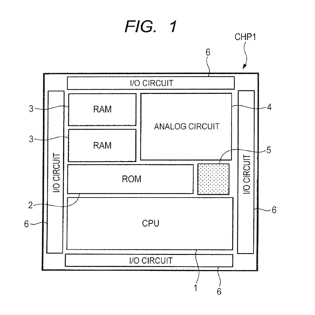
[0199]FIG. 33 shows a layout configuration example of a semiconductor chip CHP2 of Second Embodiment. In FIG. 33, the semiconductor chip CHP2 of Second Embodiment has an analog circuit 4, a nonvolatile memory 5, an I / O circuit 6, a logic circuit 7, and a driver circuit 8. The logic circuit 7 is comprised of, for example, an n channel type low breakdown voltage MISFET (n type MISFET) and a p channel type low breakdown voltage MISFET (p type MISFET), while the driver circuit 8 is comprised of, for example, an n channel type power transistor (n type power transistor) and a p channel type power transistor (p type power transistor).

[0200]The main circuit is comprised of the analog circuit 4, the logic circuit 7, and the driver circuit 8, while the add-on circuit is comprised of the nonvolatile memory 5. In short, th...


PUM


Abstract

To provide a semiconductor device having mix-loaded therein a nonvolatile memory cell and a field effect transistor at a reduced cost. A method of manufacturing a semiconductor device includes pattering a conductor film by using an additional mask that covers a gate electrode formation region of a memory formation region and exposes a main circuit formation region (field effect transistor formation region) and thereby forming a gate electrode of a nonvolatile memory cell in the memory formation region and then forming an n type semiconductor region of the nonvolatile memory cell in a semiconductor substrate by ion implantation using the above-mentioned additional mask without changing it to another one.

Description

CROSS-REFERENCE TO RELATED APPLICATIONS[0001]The disclosure of Japanese Patent Application No. 2014-172680 filed on Aug. 27, 2014 including the specification, drawings, and abstract is incorporated herein by reference in its entirety.BACKGROUND[0002]The present invention relates to a manufacturing technology of a semiconductor device, for example, a technology effective when applied to a manufacturing technology of a semiconductor device having a main circuit including a field effect transistor and a nonvolatile memory as an add-on circuit.[0003]Japanese Unexamined Patent Application Publication No. 2007-234861 (Patent Document 1) describes a technology of manufacturing a semiconductor device by forming a gate electrode of a field effect transistor and a gate electrode of a nonvolatile memory cell by respectively different steps, in which the field effect transistor and the nonvolatile memory cell can have improved reliability.[Patent Document 1] Japanese Unexamined Patent Applicati...

Claims


Application Information

Patent Timeline
Patent Type & Authority Patents(United States)
IPC IPC(8): H01L21/8238H01L29/66H01L27/11575H01L21/265H01L27/11568H01L27/112H01L23/525H01L27/11573H01L27/1157H01L21/311H01L21/266
CPCH01L27/11575H01L21/265H01L21/266H01L21/31111H01L21/31116H01L23/5256H01L27/1157H01L27/11206H01L27/11568H01L27/11573H01L29/66833H01L21/28H01L21/28008H10B69/00H01L21/26513H10B43/35H10B43/40H10B43/50H10B20/20H10B43/30
Inventor OWADA, FUKUO
Owner RENESAS ELECTRONICS CORP
Why Eureka
Try Eureka