Semiconductor electrostatic discharge protection circuit, ESD protection semiconductor device, and layout structure of ESD protection semiconductor device

a protection circuit and semiconductor technology, applied in the field of electrostatic discharge, can solve the problems of not being able being more vulnerable to the impact of external environment, and being unable to provide protection to the internal circuit, etc., to achieve the effect of reducing the trigger voltage, increasing the holding current, and reducing the holding curren

Active Publication Date: 2017-07-25
UNITED MICROELECTRONICS CORP
View PDF4 Cites 7 Cited by
  • Summary
  • Abstract
  • Description
  • Claims
  • Application Information

AI Technical Summary

Benefits of technology

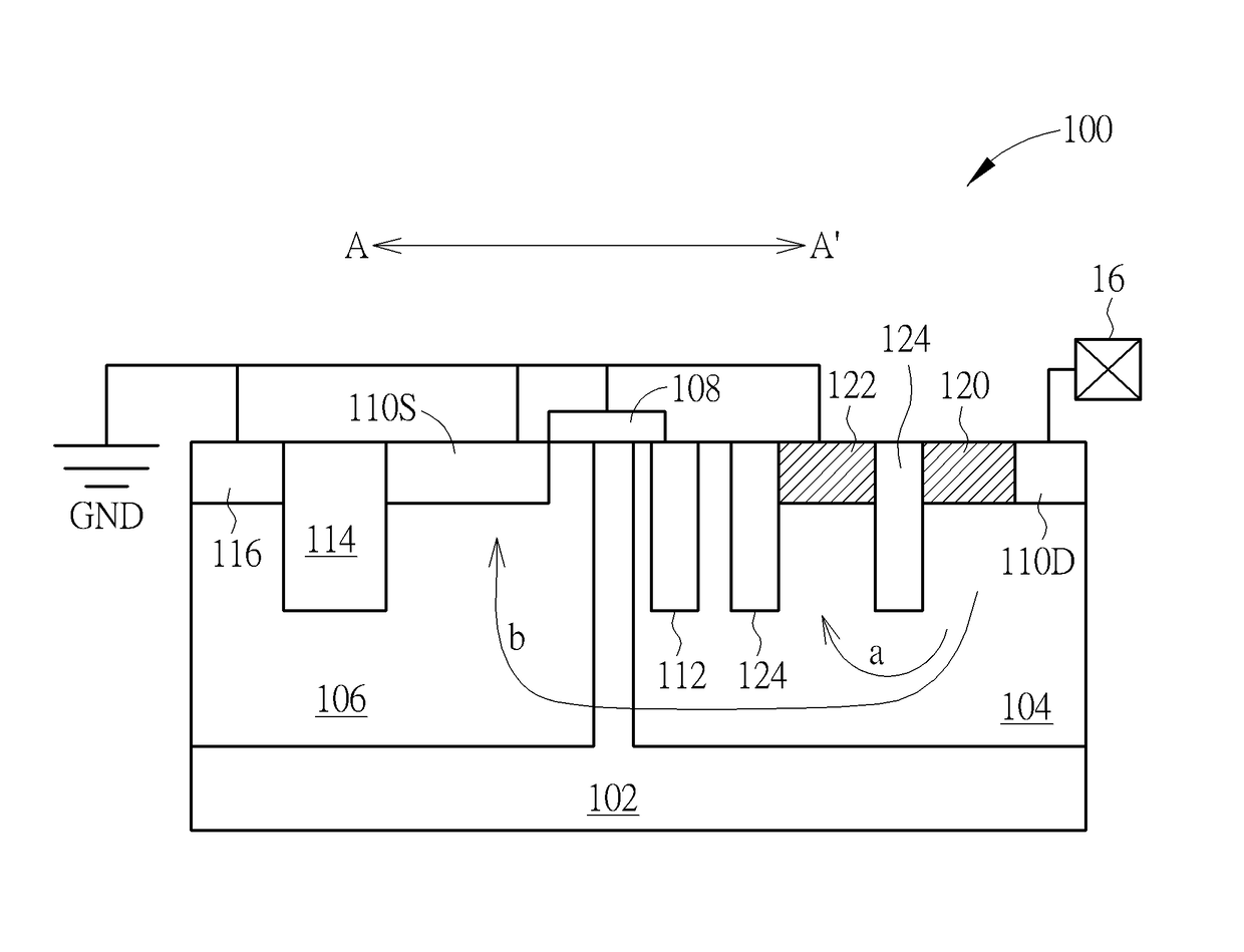
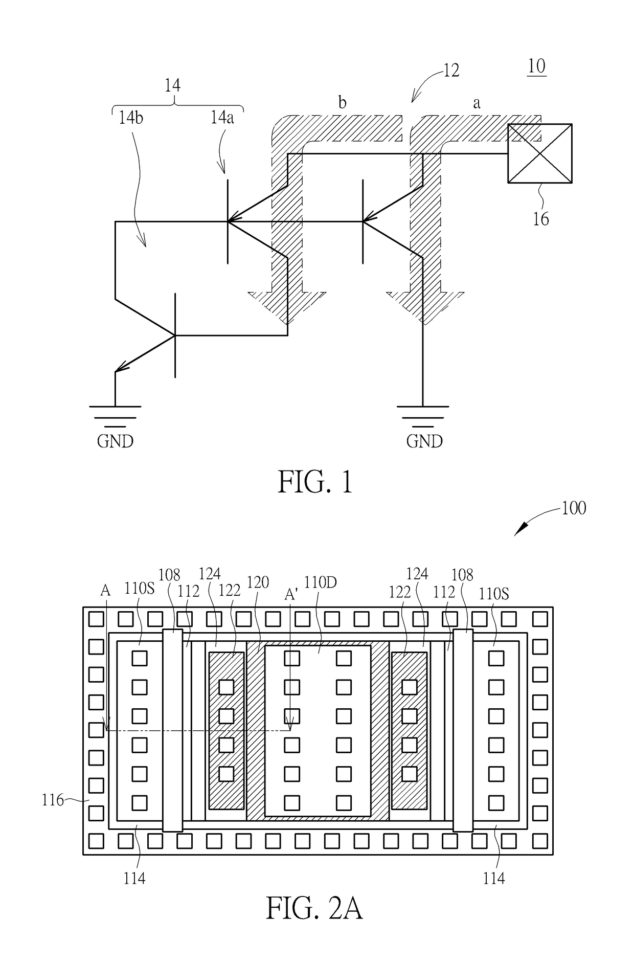
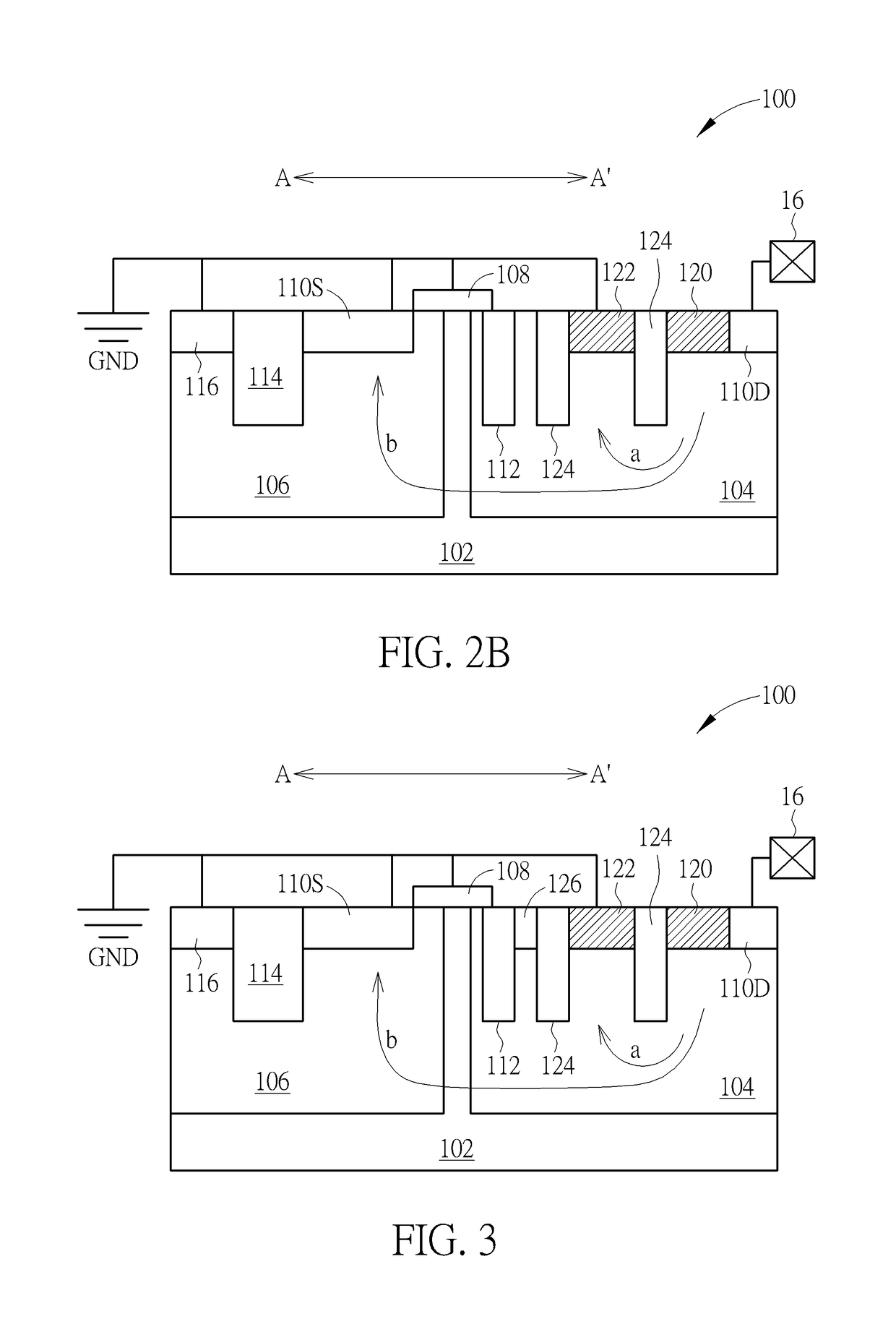
[0010]According to the ESD protection semiconductor device and the layout structure of the ESD protection semiconductor device provided by the present invention, the first doped region and the second doped region, which are both formed in the first well and include conductivity type complementary to the first well are provided. Thus, a parasite BJT is formed by the first doped region, the first well and the second doped region. Furthermore, a SCR is formed by the first doped region, the first well, the second well and the source region. The SCR is electrically connected to the BJT in parallel and thus an ESD protection circuit is obtained. More important, the BJT is always turned on before the SCR in an ESD event. Therefore a portion of the ESD current is bypassed by the BJT. When the voltage is increased, the SCR is then turned on, and thus the holding current of the ESD protection circuit is significantly increased. According to the ESD protection circuit, the ESD protection semiconductor device and the layout structure of the ESD protection semiconductor device provided by the present invention, higher holding current and lower trigger voltage are obtained, and latch-up immunity is consequently improved without increasing layout area.

Problems solved by technology

As products based on ICs become more delicate, they also become more vulnerable to the impacts from external environment.
And thus, it is assumed that ESD is a constant threat to the modern electronics.
However, a problem arises when the holding voltage is lower than the operating voltage (Vdd) at which the ESD protection device / circuit operates: it is easily latched-up and thus cannot provide protection to the internal circuit.

Method used


Image

  • Semiconductor electrostatic discharge protection circuit, ESD protection semiconductor device, and layout structure of ESD protection semiconductor device
  • Semiconductor electrostatic discharge protection circuit, ESD protection semiconductor device, and layout structure of ESD protection semiconductor device
  • Semiconductor electrostatic discharge protection circuit, ESD protection semiconductor device, and layout structure of ESD protection semiconductor device

Examples


Embodiment Construction

[0021]In the following description, numerous specific details are set forth, such as particular structures, components, materials, dimensions, processing steps and techniques, in order to provide a thorough understanding of the present invention. However, it will be appreciated by one of ordinary skill in the art that the invention may be practiced without these specific details. In other instances, well-known structures or processing steps have been described in detail in order to avoid obscuring the invention.

[0022]It will be understood that when an element is referred to as being “formed” on another element, it can be directly or indirectly, formed on the given element by growth, deposition, etch, attach, connect, or couple. And it will be understood that when an elements or a layer is referred to as being “on”, “connected to”, or “coupled to” another element or layer, it can be directly on, connected or coupled to the other element or layer or intervening elements or layers may ...


PUM


Abstract

An electrostatic discharge protection semiconductor device includes a substrate, a first well formed in the substrate, a second well formed in the substrate and spaced apart from the first well, a gate formed on the substrate and positioned in between the first well and the second well, a drain region formed in the first well, a source region formed in the second well, a first doped region formed in the first well and adjacent to the drain region, and a second doped region formed in the first well and spaced apart from both the first doped region and the gate. The first well, the drain region, and the source region include a first conductivity type, the second well, the first doped region and the second doped region include a second conductivity type, and the first conductivity type and the second conductivity type are complementary to each other.

Description

BACKGROUND OF THE INVENTION[0001]1. Field of the Invention[0002]The present invention relates to an electrostatic discharge (hereinafter abbreviated as ESD) protection circuit, an ESD protection semiconductor device, and a layout structure of an ESD protection semiconductor device, and more particularly, to an ESD protection circuit including an ESD protection semiconductor device and a layout structure of the ESD protection semiconductor device.[0003]2. Description of the Prior Art[0004]With the advancement of technology, the development of semiconductor process is ongoing. A modern chip is therefore allowed to have a plurality of various electronic circuits configured within. For example, the integrated circuits (hereinafter abbreviated as ICs) integrated in the chip(s) can be divided into core circuits and input / output (hereinafter abbreviated as I / O) circuits, and the core circuits and the I / O circuits are respectively driven by different power supply sources with different volt...

Claims


Application Information

Patent Timeline
Patent Type & Authority Patents(United States)
IPC IPC(8): H01L27/02
CPCH01L27/0262
Inventor HUANG, CHUNG-YUTANG, TIEN-HAO
Owner UNITED MICROELECTRONICS CORP
Why Eureka
Try Eureka