Thin film electronic component

a technology of electronic components and thin films, applied in semiconductor devices, semiconductor/solid-state device details, capacitors, etc., can solve the problems of physical stress, inability to adequately maintain impact resistance and moisture resistance properties, and degradation of certain electric properties, so as to improve the impact resistance properties and moisture resistance properties of electronic components. , physical stress can be prevented

Active Publication Date: 2017-08-01
TAIYO YUDEN KK
View PDF6 Cites 0 Cited by
  • Summary
  • Abstract
  • Description
  • Claims
  • Application Information

AI Technical Summary

Benefits of technology

[0012]An object of the present invention is to provide a thin film electronic component with excellent impact-resistance and water-resistance properties.
[0016]According to the above-described aspect of the present invention, physical stress can be prevented from becoming concentrated since the shape of the borderline defining the through-hole at a top surface of the organic insulation layer in a plan view has chamfered corners. This allows for improvements in both impact-resistance properties and moisture-resistance properties.
[0023]According to at least some aspects of the present invention, physical stress can be prevented from becoming concentrated in the formation location of the lead-out electrode in the organic insulation layer, which allows for improvements in the impact-resistance properties and the moisture-resistance properties of the electronic component.

Problems solved by technology

There have been some problems with the structure of conventional thin film electronic components, depending on the specific shape, material, mounting conditions, and the like of the various parts.
These problems include not being able to adequately maintain the impact-resistance and moisture-resistance properties, and degradation of certain electric properties and, especially in the case of thin film capacitors, capacitance properties.
When the organic resin film absorbs moisture from the surrounding environment and expands, there is the possibility that stress may be generated.
In addition, in thin film electronic components in which materials with different thermal expansion coefficients have been stacked, there is the possibility that significant structural stress will occur and lead to structural problems such as cracks and parts becoming detached.
There is also the possibility that the lead-out electrode will become detached as a result of cracks forming in the barrier layer and the protective insulation layer due to stress.
This may lead to moisture entering the component at locations where the lead-out electrode meets the barrier layer and the protective insulation layer, which may result in a degradation of the properties of the thin film capacitor.

Method used


Image

  • Thin film electronic component
  • Thin film electronic component
  • Thin film electronic component

Examples


Embodiment Construction

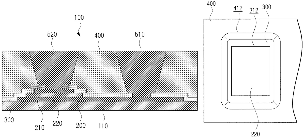
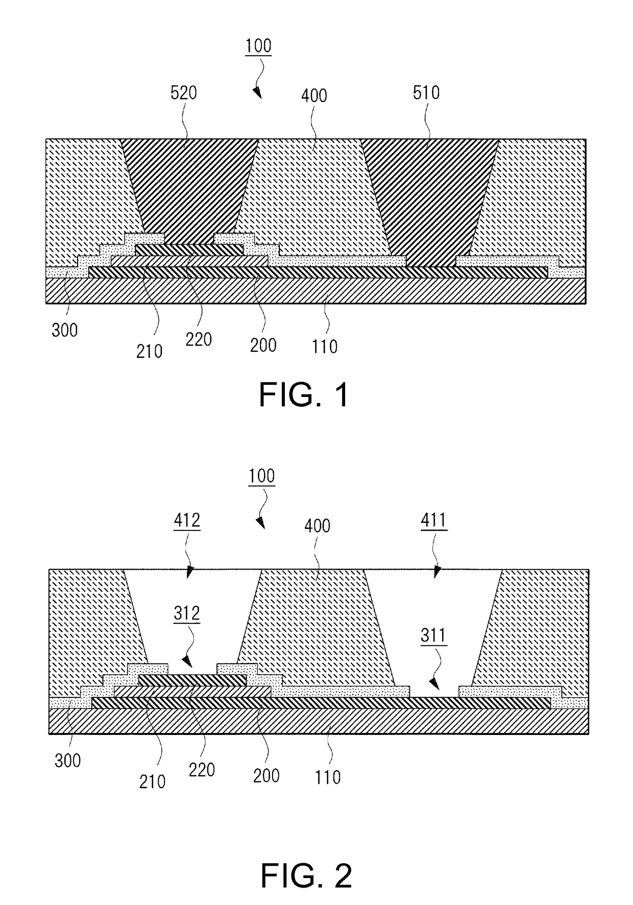
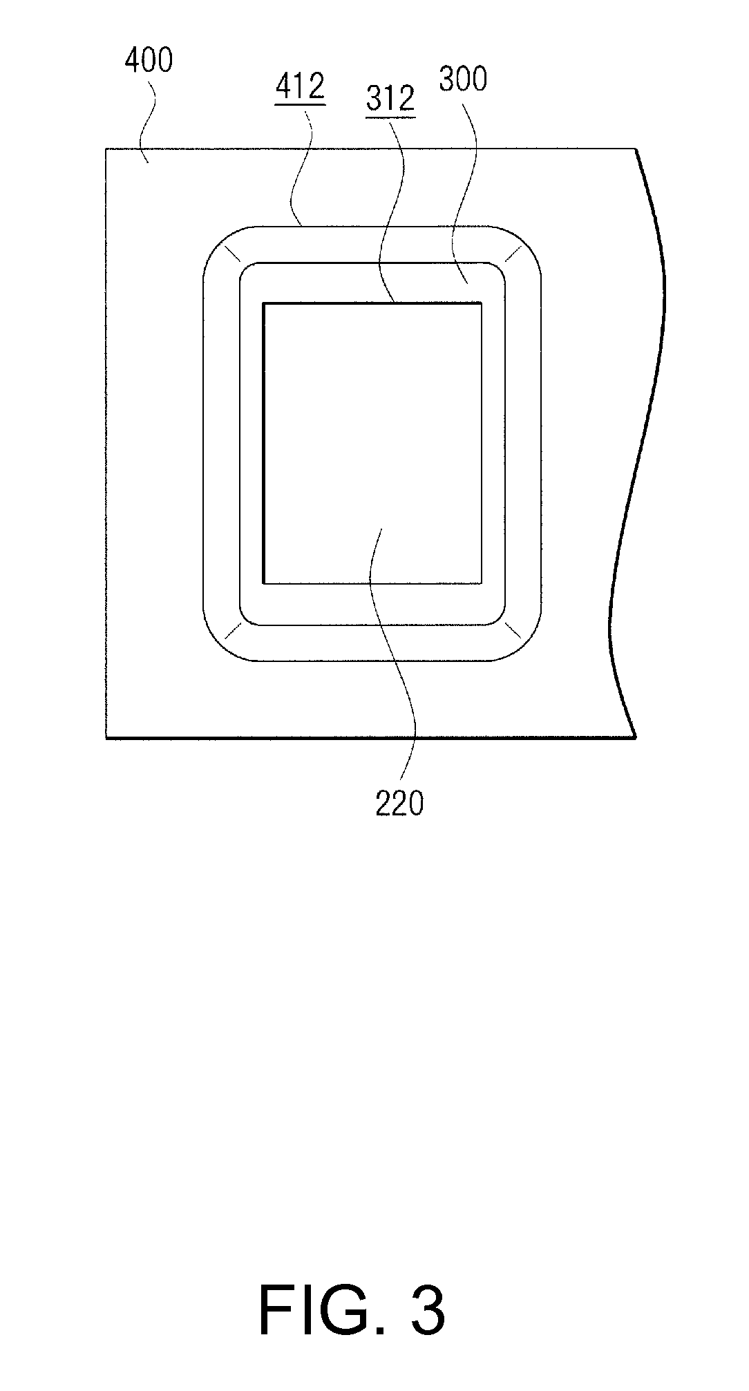
[0033]A thin film electronic component according to an embodiment of the present invention will be explained with reference to the drawings. A thin film capacitor will be described in the present embodiment. FIG. 1 is a cross-section of a thin film capacitor, FIG. 2 is a cross-section of the thin film capacitor in which the lead-out electrode has been removed, and FIG. 3 is a plan view of the thin film capacitor in which the lead-out electrode has been removed. It should be noted that these various figures are schematic representations used to describe the invention and are not shown to scale.

[0034]As shown in FIG. 1, a thin film capacitor 100 includes: a supporting substrate 110; a first electrode layer 200 formed on the supporting substrate 110; a dielectric layer 210 formed on the first electrode layer; a second electrode layer 220 formed on the dielectric layer 210; a barrier layer 300 formed so as to cover the first electrode layer 200, the dielectric layer 210, the second elec...


PUM

PropertyMeasurementUnit
temperatureaaaaaaaaaa
bending angleaaaaaaaaaa
thicknessaaaaaaaaaa

Abstract

A thin film electronic component includes: a substrate; a thin film electrode layer over the substrate; an inorganic insulation layer formed on the thin film electrode layer; an organic insulation layer formed on the inorganic insulation layer; and a lead-out electrode that electrically connects to the thin film electrode layer. The inorganic insulation layer has a through-hole formed therein, so as to expose a portion of the thin film electrode layer. The organic insulation layer has a through-hole formed therein, so as to expose the through-hole in the inorganic insulation layer. The lead-out electrode is formed in the through-hole in the inorganic insulation layer and the through-hole in the organic insulation layer. A shape of a borderline defining the through-hole at a top surface of the organic insulation layer in a plan view has chamfered corners.

Description

BACKGROUND OF THE INVENTION[0001]Technical Field[0002]The present invention relates to a thin film electronic component that constitutes a prescribed functional component. The component is created by forming a conductive layer and an insulation layer on a supporting substrate via a thin film fabrication process.[0003]Background Art[0004]Thin film capacitors are one well-known type of this type of thin film electronic component (see Patent Document 1, for example). This kind of thin film capacitor includes: a supporting substrate such as a silicon substrate; a capacitance section formed of a metallic thin film electrode such as platinum and a dielectric layer that is made up of a metal oxide formed via a thin film fabrication process such as sputtering; a protective insulation layer formed of an organic resin film that covers the entire silicon supporting substrate, which includes the capacitance section; a barrier layer that is made up of a non-conductive inorganic material and that...

Claims


Application Information

Patent Timeline
Patent Type & Authority Patents(United States)
IPC IPC(8): H01L23/48H01L21/768H01L49/02H01L27/02
CPCH01L28/60H01L21/76816H01L28/40H01L27/0207H01L2924/0002H01L2924/00
Inventor MORITO, KENTAROISHII, DAIKI
Owner TAIYO YUDEN KK
Why Eureka
Try Eureka