Semiconductor device, memory device, electronic device, or method for driving the semiconductor device

a semiconductor device and memory technology, applied in semiconductor/solid-state device testing/measurement, semiconductor/solid-state device details, instruments, etc., can solve problems such as increasing circuit size, and achieve the effect of reducing circuit size, introducing a new driving method of a semiconductor device, and large data storage capacity

Inactive Publication Date: 2017-09-26
SEMICON ENERGY LAB CO LTD
View PDF255 Cites 7 Cited by
  • Summary
  • Abstract
  • Description
  • Claims
  • Application Information

AI Technical Summary

Benefits of technology

[0013]To execute addition or subtraction processing, the data retained in the memory cell needs to be converted into a digital value; therefore, it takes time to execute addition or subtraction processing after reading. In addition, it is necessary to separately provide a functional block for executing addition or subtraction processing, which may increase the circuit size.
[0015]Another object of one embodiment of the present invention is to provide a memory device with large data storage capacity. Another object of one embodiment of the present invention is to provide a miniaturized memory device. Another object of one embodiment of the present invention is to provide a memory device with a decreased circuit size. Another object of one embodiment of the present invention is to provide a memory device capable of maintaining stored data without any change. Another object of one embodiment of the present invention is to provide a memory device with low power consumption or a driving method of the memory device. Another object of one embodiment of the present invention is to provide a memory device in which a time needed for a reading operation and addition or subtraction processing is short, or a driving method of the memory device.
[0025]According to one embodiment of the present invention, a memory device with large data storage capacity can be provided. According to one embodiment of the present invention, a miniaturized memory device can be provided. According to one embodiment of the present invention, a memory device with a decreased circuit size can be provided. According to one embodiment of the present invention, a memory device capable of maintaining stored data without any change can be provided. According to one embodiment of the present invention, a memory device with low power consumption or a driving method of the memory device can be provided. According to one embodiment of the present invention, a memory device in which a time needed for a reading operation and addition or subtraction processing is short, or a driving method of the memory device can be provided.

Problems solved by technology

In addition, it is necessary to separately provide a functional block for executing addition or subtraction processing, which may increase the circuit size.

Method used


Image

  • Semiconductor device, memory device, electronic device, or method for driving the semiconductor device
  • Semiconductor device, memory device, electronic device, or method for driving the semiconductor device
  • Semiconductor device, memory device, electronic device, or method for driving the semiconductor device

Examples


embodiment 1

[0065]In this embodiment, an example of a semiconductor device of the disclosed invention is described.

Configuration Example

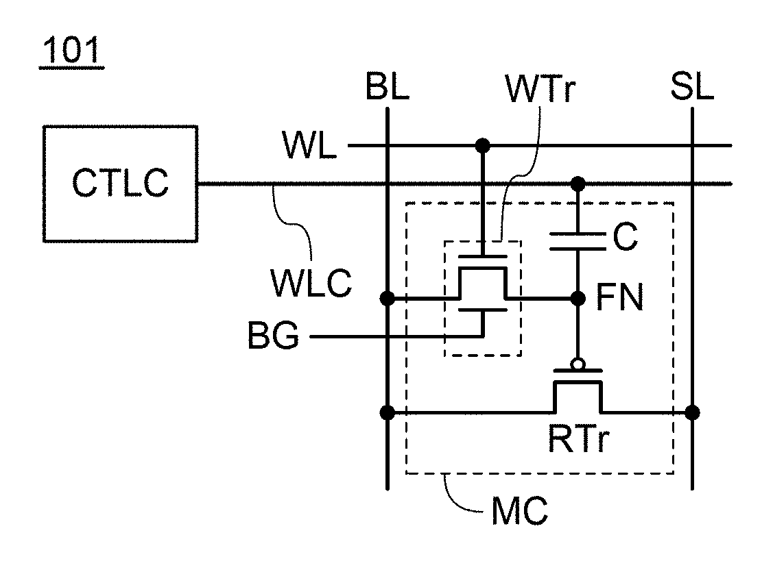
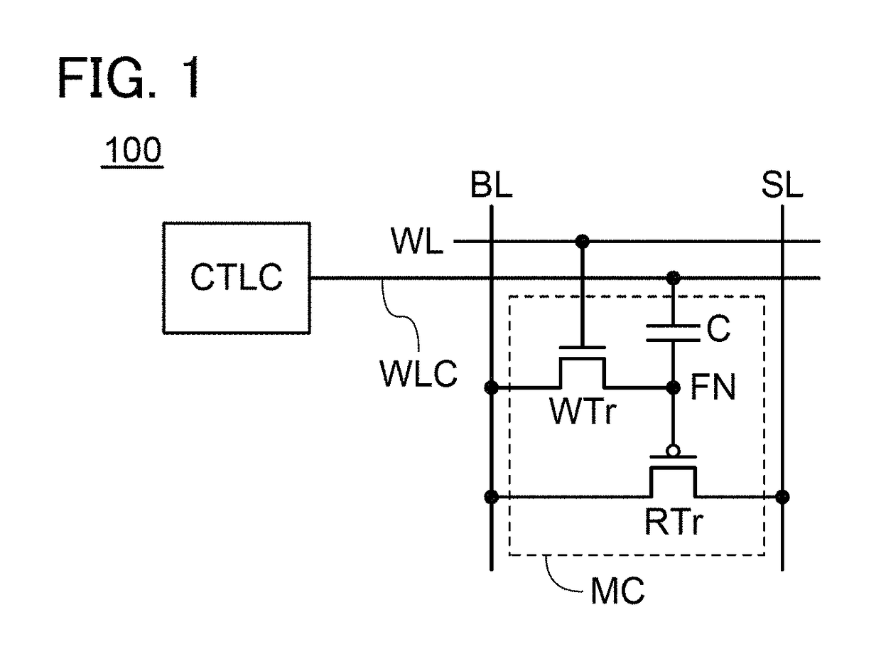
[0066]FIG. 1 shows an example of a semiconductor device of one embodiment of the present invention. A semiconductor device 100 includes a memory cell MC and a control circuit CTLC. The memory cell MC includes a transistor WTr, a transistor RTr, and a capacitor C. Note that the transistor WTr is an n-channel transistor, and the transistor RTr is a p-channel transistor.

[0067]The memory cell MC is electrically connected to a wiring BL, a wiring SL, a wiring WL, and a wiring WLC.

[0068]A first terminal of the transistor WTr is electrically connected to a first terminal of the capacitor C and a gate of the transistor RTr via a retention node FN. A second terminal of the transistor WTr is electrically connected to the wiring BL, and a gate of the transistor WTr is electrically connected to the wiring WL. A first terminal of the transistor RTr is electrically connected...

operation example

[0088]Next, the operation of the semiconductor device 100 of one embodiment of the present invention is described. FIG. 4 and FIGS. 5A and 5B are timing charts each showing an operation example of the semiconductor device 100.

>

[0089]First, an example of a writing operation of the semiconductor device 100 is described. For writing of data to the memory cell MC, a high-level potential is applied to the wiring WL to turn on the transistor WTr. After that, a writing bit signal is input to the wiring BL to write the writing bit signal to the retention node FN via the transistor WTr. Finally, a low-level potential is applied to the wiring WL to turn off the transistor WTr, so that writing of data to the memory cell MC is completed. It is preferable that the potential of the wiring WLC be a reference potential continuously.

[0090]FIG. 4 is a timing chart showing an example of the operation for writing data to the semiconductor device 100. FIG. 4 demonstrates changes in the potentials of the...

embodiment 2

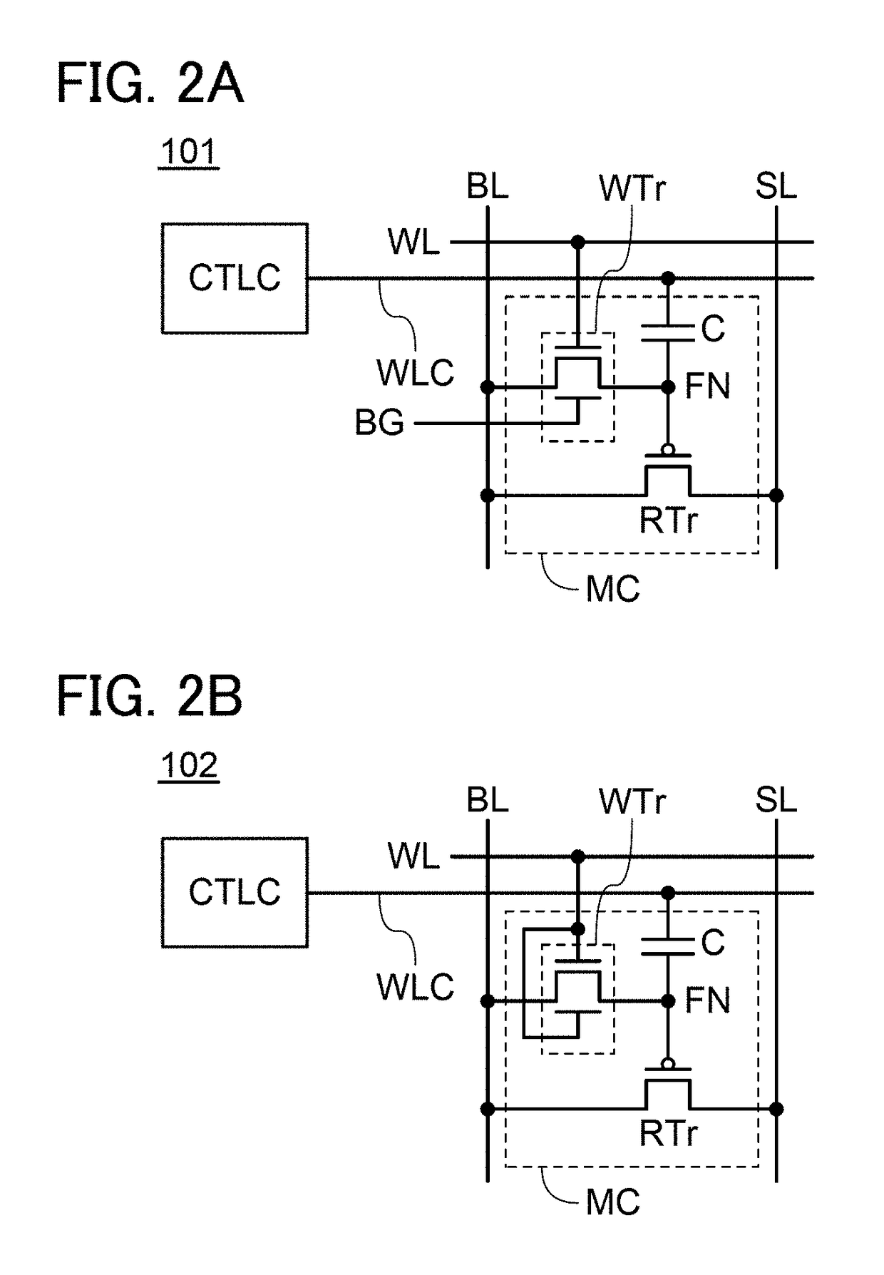
[0135]In this embodiment, a configuration of a semiconductor device which is different from that of the semiconductor device 100 described in Embodiment 1 is described.


PUM


Abstract

A semiconductor device with an improved arithmetic processing speed and a decreased circuit size, and its driving method are provided. In the semiconductor device, a first terminal of a first transistor and a gate of a second transistor are electrically connected to a first terminal of a capacitor, and a control circuit is electrically connected to a second terminal of the capacitor. The control circuit supplies a first potential to the second terminal of the capacitor, in other words, adds a value corresponding to the first potential to the value of first data previously retained in the gate of the second transistor in order to obtain second data. In the second transistor, the second data, specifically, a third potential commensurate with the potential of the gate will be output from a second terminal when a second potential is supplied to a first terminal.

Description

BACKGROUND OF THE INVENTION[0001]1. Field of the Invention[0002]One embodiment of the present invention relates to a semiconductor device, a memory device, an electronic device, or a driving method of the semiconductor device.[0003]Note that one embodiment of the present invention is not limited to the above technical field. The technical field of the invention disclosed in this specification and the like relates to an object, a method, or a manufacturing method. In addition, one embodiment of the present invention relates to a process, a machine, manufacture, or a composition of matter. Specifically, examples of the technical field of one embodiment of the present invention disclosed in this specification include a semiconductor device, a display device, a liquid crystal display device, a light-emitting device, a power storage device, an imaging device, a memory device, a processor, an electronic device, a method for driving any of them, a method for manufacturing any of them, a me...

Claims


Application Information

Patent Timeline
Patent Type & Authority Patents(United States)
IPC IPC(8): G11C5/06G06K19/077G11C11/419G11C5/10H01L23/31H01L23/544H01L21/66H01L23/495H01L21/56H01L23/00H01L21/48H01L21/78H01L29/786H01L27/12H01L27/105
CPCH01L27/1052G06K19/07749G11C5/063G11C5/10G11C11/419H01L21/4825H01L21/565H01L21/78H01L22/14H01L23/3114H01L23/4952H01L23/49555H01L23/544H01L24/45H01L24/48H01L27/124H01L27/127H01L27/1225H01L27/1255H01L29/7869H01L29/78606H01L29/78648H01L29/78651H01L29/78696H01L2223/54486H01L2224/45139H01L2224/45144H01L2224/48245H01L2224/48453H01L2224/48458G11C11/565H01L2924/00014H01L28/00H10B43/27H01L2224/05599H01L2224/85399H10B99/00
Inventor MATSUZAKI, TAKANORI
Owner SEMICON ENERGY LAB CO LTD
Why Eureka
Try Eureka