Metrology tool with combined XRF and SAXS capabilities

a technology of saxs and saxs, applied in the field of metalrology systems and methods, can solve the problems of difficult characterization, inability to reliably decouple parameters characterizing the target with available measurements, and difficulty in characterization, so as to improve the precision and accuracy of parameters measured with combined saxs and saxs techniques, reduce correlations among parameters, and improve measurement accuracy

Active Publication Date: 2017-10-03
KLA CORP
View PDF25 Cites 26 Cited by
  • Summary
  • Abstract
  • Description
  • Claims
  • Application Information

AI Technical Summary

Benefits of technology

[0011]In another aspect, the precision and accuracy of parameters measured with combined SAXS and XRF techniques is improved by identifying shared model parameters that can be mathematically resolved using data sets derived from SAXS and XRF measurements either sequentially or in parallel. Measuring shared parameters with a diversity of measurement technologies reduces correlations among parameters and improves measurement accuracy.
[0012]In yet another aspect, SAXS measurements performed on a planar specimen (e.g., semiconductor wafer) oriented at a number of different out of plane orientations increases the precision and accuracy of measured parameters. Measuring a location of the specimen at a number of different angles results in an enhanced data set corresponding to that location. Measuring parameters with a deeper, more diverse data set also reduces correlations among parameters and improves measurement accuracy.

Problems solved by technology

As devices (e.g., logic and memory devices) move toward smaller nanometer-scale dimensions, characterization becomes more difficult.
Devices incorporating complex three-dimensional geometry and materials with diverse physical properties contribute to characterization difficulty.
For example, modern memory structures are often high-aspect ratio, three-dimensional structures that make it difficult for XRF radiation to penetrate to the bottom layers.
As a result, the parameters characterizing the target often cannot be reliably decoupled with available measurements.
XRF radiation is often unable to penetrate layers constructed of these materials.
As a result, measurements with thin-film scatterometry tools such as ellipsometers or reflectometers are becoming increasingly challenging.
However, these approaches have not reliably overcome fundamental challenges associated with measurement of many advanced targets (e.g., complex 3D structures, structures smaller than 10 nm, structures employing opaque materials) and measurement applications (e.g., line edge roughness and line width roughness measurements).
Although large spot sizes can be mitigated using, for example, apertures or knife edges, this results in an undesirable reduction in flux and increase in measurement time.
Future metrology applications present challenges for metrology due to increasingly small resolution requirements, multi-parameter correlation, increasingly complex geometric structures, and increasing use of opaque materials.

Method used


Image

  • Metrology tool with combined XRF and SAXS capabilities
  • Metrology tool with combined XRF and SAXS capabilities
  • Metrology tool with combined XRF and SAXS capabilities

Examples


Embodiment Construction

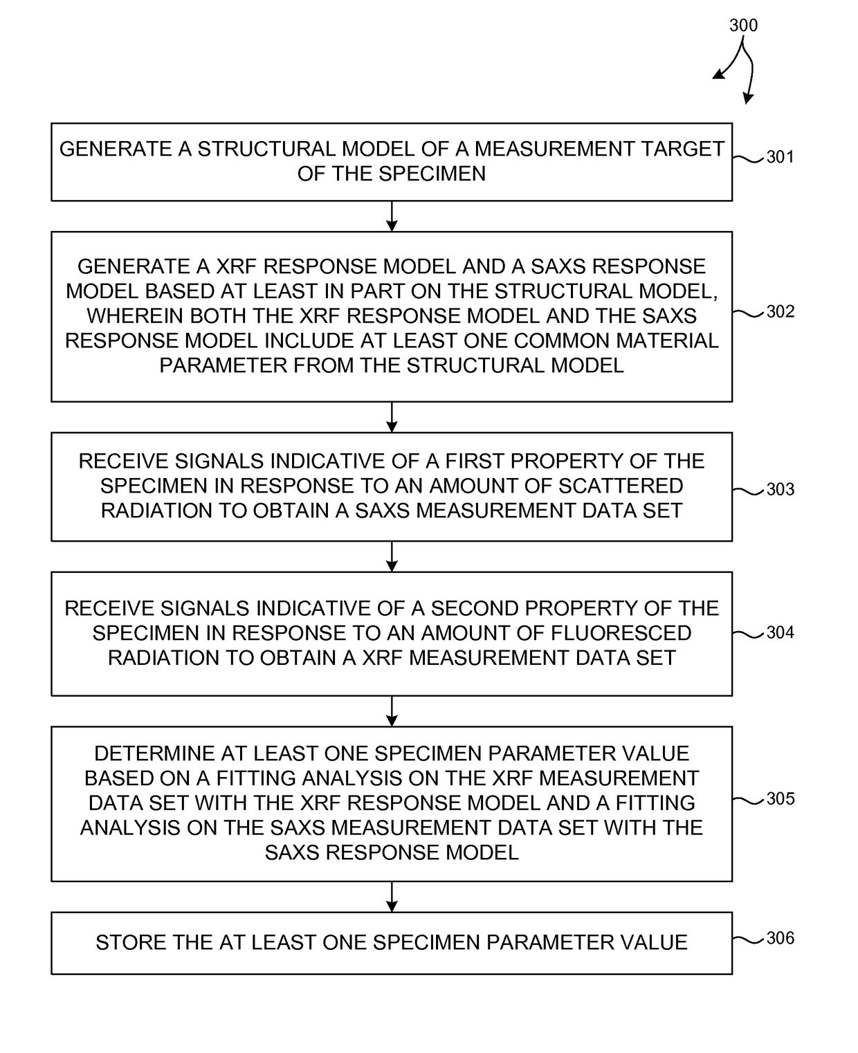
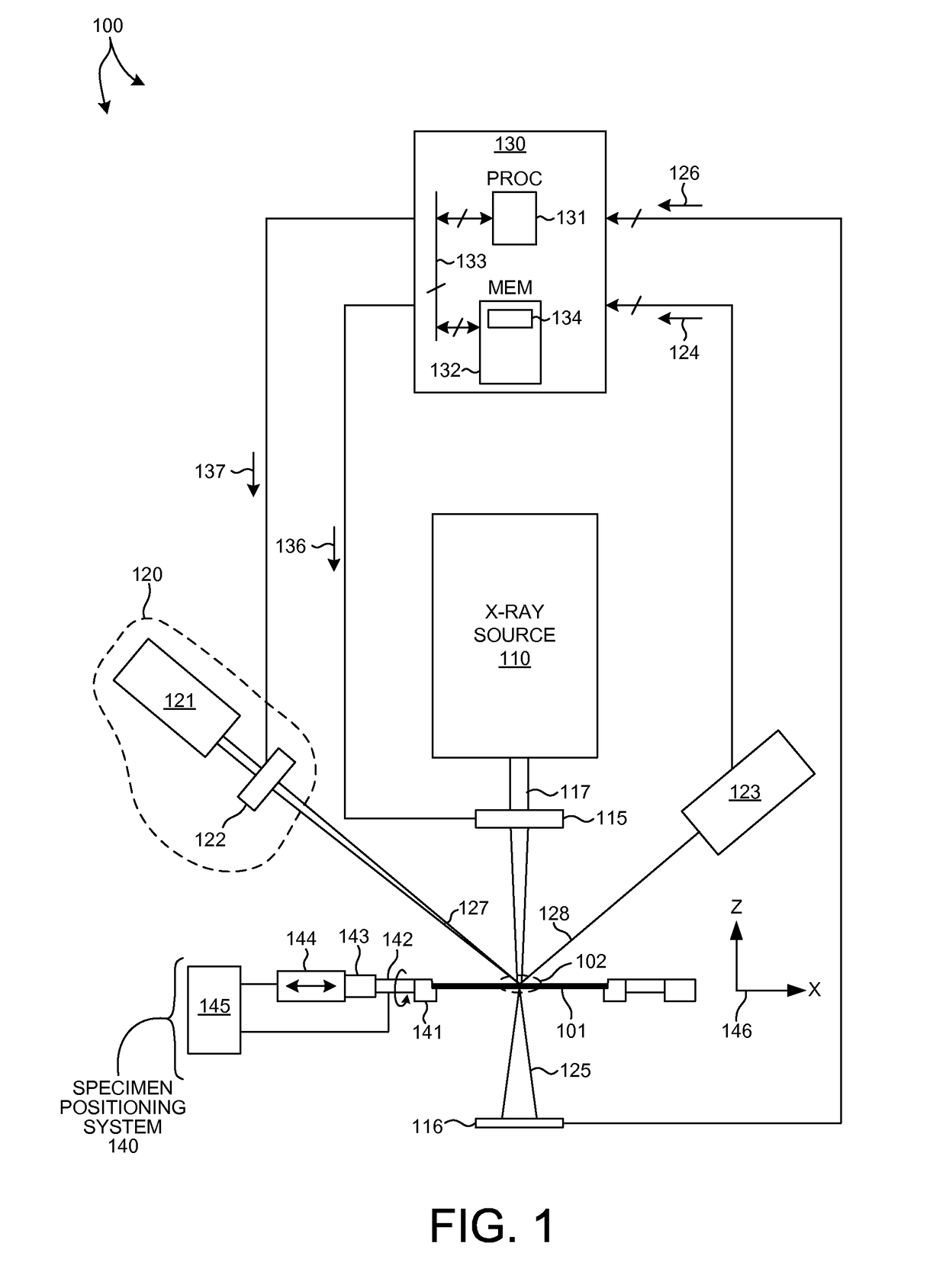
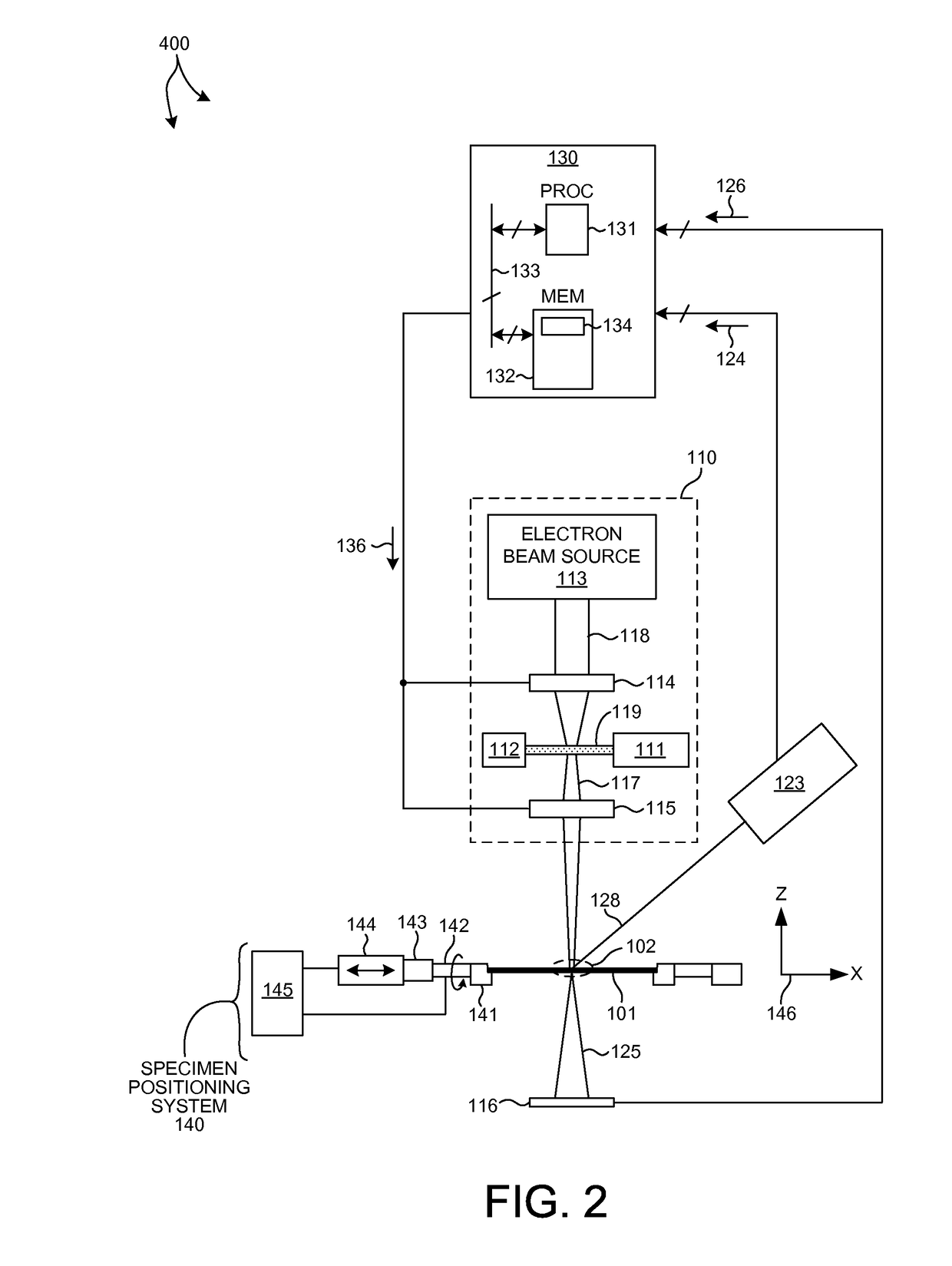
[0020]Reference will now be made in detail to background examples and some embodiments of the invention, examples of which are illustrated in the accompanying drawings. Methods and systems for performing measurements of semiconductor structures and materials with a combination of Small-Angle X-Ray Scattering (SAXS) and X-Ray Fluorescence (XRF) measurement modalities are presented. Such systems are employed to measure structural and material characteristics (e.g., material composition, dimensional characteristics of structures and films, etc.) associated with different semiconductor fabrication processes.

[0021]The combined use of XRF and high brightness SAXS (in either grazing incidence or transmission incidence configurations) enables high flux x-ray radiation penetration into opaque areas of the target. Examples of measureable geometric parameters using combined SAXS and XRF include pore size, pore density, line edge roughness, line width roughness, side wall angle, profile, film t...


PUM

PropertyMeasurementUnit
roughnessaaaaaaaaaa
line edge roughnessaaaaaaaaaa
sizeaaaaaaaaaa

Abstract

Methods and systems for performing simultaneous X-ray Fluorescence (XRF) and small angle x-ray scattering (SAXS) measurements over a desired inspection area of a specimen are presented. SAXS measurements combined with XRF measurements enables a high throughput metrology tool with increased measurement capabilities. The high energy nature of x-ray radiation penetrates optically opaque thin films, buried structures, high aspect ratio structures, and devices including many thin film layers. SAXS measurements of a particular location of a planar specimen are performed at a number of different out of plane orientations. This increases measurement sensitivity, reduces correlations among parameters, and improves measurement accuracy. In addition, specimen parameter values are resolved with greater accuracy by fitting data sets derived from both SAXS and XRF measurements based on models that share at least one material parameter. The fitting can be performed sequentially or in parallel.

Description

CROSS REFERENCE TO RELATED APPLICATION[0001]The present application for patent claims priority under 35 U.S.C. §119 from U.S. provisional patent application Ser. No. 61 / 867,404, entitled “Metrology Apparatus with SAXS and XRF Capabilities,” filed Aug. 19, 2013, the subject matter of which is incorporated herein by reference in its entirety.TECHNICAL FIELD[0002]The described embodiments relate to metrology systems and methods, and more particularly to methods and systems for improved measurement accuracy.BACKGROUND INFORMATION[0003]Semiconductor devices such as logic and memory devices are typically fabricated by a sequence of processing steps applied to a specimen. The various features and multiple structural levels of the semiconductor devices are formed by these processing steps. For example, lithography among others is one semiconductor fabrication process that involves generating a pattern on a semiconductor wafer. Additional examples of semiconductor fabrication processes inclu...

Claims


Application Information

Patent Timeline
Patent Type & Authority Patents(United States)
IPC IPC(8): G06F17/50G01N23/201G01N23/223
CPCG01N23/223G01N23/201G01N2223/6116
Inventor BAKEMAN, MICHAEL S.SHCHEGROV, ANDREI V.PETERLINZ, KEVINDZIURA, THADDEUS GERARD
Owner KLA CORP
Why Eureka
Try Eureka