Low power nanoelectronics

a nanoelectronics and low-power technology, applied in the direction of transformers, semiconductor devices, inductances, etc., can solve the problems of additional biological infection risk, limited computational capability, and limited operational range of existing rf-powered systems, so as to increase the power efficiency and power efficiency of these components.

Active Publication Date: 2017-10-24
PENN STATE RES FOUND
View PDF1 Cites 1 Cited by
  • Summary
  • Abstract
  • Description
  • Claims
  • Application Information

AI Technical Summary

Benefits of technology

[0007]Tunneling Field Effect Transistor (“TFET”) and Hetero-junction Tunnel FET (“HTFET”) for ultra-low power RF circuit design have been explored at the device and circuit level. Our evaluation of a TFET-based RF-power harvesting and signal processing components demonstrates their ability to increase PCE and power efficiencies of these components, as compared to other RF-power harvesting and signal processing components (e.g., CMOS).
[0008]Disclosed is a TFET-based rectifier configured with various topologies, wherein steep-slope switching of the HTFET may be used to reduce the VCC window, and the high on-current Ion of the HTFET at low voltage may be used to reduce on-state channel resistance to achieve increased power out and power conversion efficiency. In one embodiment of a HTFET based ultra-low power high sensitivity RF rectifier, demonstrated through device-circuit simulation, a 10-stage optimized HTFET RF rectifier operates at 915 MHz with a power conversion efficiency of 98% with 0.5 nW Dc power consumption, sensitivity of −24 dBm for 9 μW of DC output power, and sensitivity of −33 dBm for 0.4 μW DC output power. The capability of obtaining a high PCE at a low RF input power range demonstrates the ability of HTFET RF rectifiers to enhance battery-less energy harvesting applications.
[0010]Also disclosed is a TFET-based amplifier including a telescopic operational transconductance amplifier topology (OTA). The steep slope switching of a HTFET may be used to increase gm / Ids to achieve an increase in gain at low supply voltage. In one embodiment, the high gm / Ids characteristics may be used in a HTFET-based neural amplifier with a shared telescopic OTA topology to enable a nanowatt power-level operation, which also provides a significant voltage gain improvement and noise reduction compared to prior art. At a highly scaled bias current of 10 nA and supply voltage of 0.5 V, the HTFET-based neural amplifier may exhibit a midband gain of 40 dB, a −3 dB bandwidth from 12 Hz to 2 kHz, and an approximate 32 times power reduction over the prior art at the same input-referred noise level. The HTFET-based neural amplifier also exhibits improved power-noise efficiency, including a noise efficiency factor (NEF) of 0.64.
[0011]Also disclosed is a TFET-based successive-approximation register (SAR) analog-to-digital (A / D) converter, including a HTFET-based transmission gate flip-flop (DFF). The steep slope switching of a HTFET may be used to increase gm / Ids, increase signal-to-noise and distortion (SNDR), increase effective number of bits (ENOB), lower the energy per conversion step figure-of-merit (FoM), and lower the energy consumption. The HTFET-based SAR A / D converter demonstrates a 1.94 dB higher SNDR, a 0.32-bit larger ENOB, a 63% lower average power consumption, and a 35% lower energy per conversion-step (FoM) as compared to prior art. This performance advantage stems from increasing current strength due to steep slope transistor characteristics and transistor size reduction, which is desirable for ultra-low-power A / D Converters at supply voltage VDD<0.50 V.
[0012]Also disclosed is an RF-powered system including at least one of the TFET-based devices described above. RF-powered systems including at least one of the HTFET-based devices described above may be used to improve the power conversion efficiencies of power harvesters within the power harvesting and management block of the RF-powered system and / or improve the power-efficiency of signal processing components of the analog / RF front end and digital storage / processing block of the RF-powered system.

Problems solved by technology

Use of RF-power harvester circuits may also obviate the inconvenience of charging or replacing the stored energy source.
With biomedical applications (e.g., medical implants), chemical leakage may pose an additional biological infection risk, thus omission of batteries in these systems may reduce such risk.
Existing RF-powered systems have limited operational range and computational capability due to the limited ambient RF power that can be harvested from the ambient environment.
One of the reasons for this is the low power-conversion efficiency (PCE) of energy scavenging components of the RF-powered system when attempting to harvest power from the limited ambient RF power.
Furthermore, their sensing, identification, and / or transmission functions may have to be abridged due to the limited ambient RF power.

Method used


Image

  • Low power nanoelectronics
  • Low power nanoelectronics
  • Low power nanoelectronics

Examples


Embodiment Construction

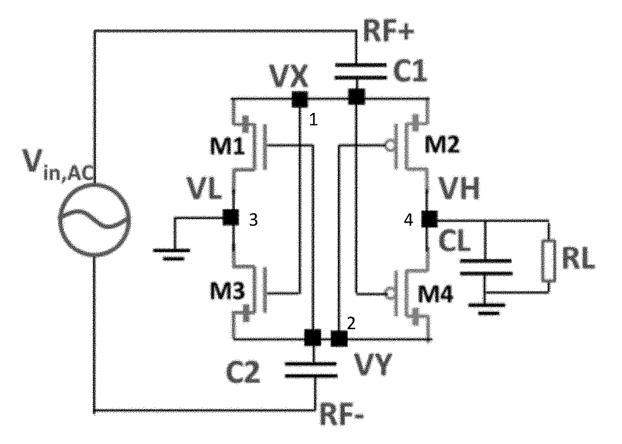
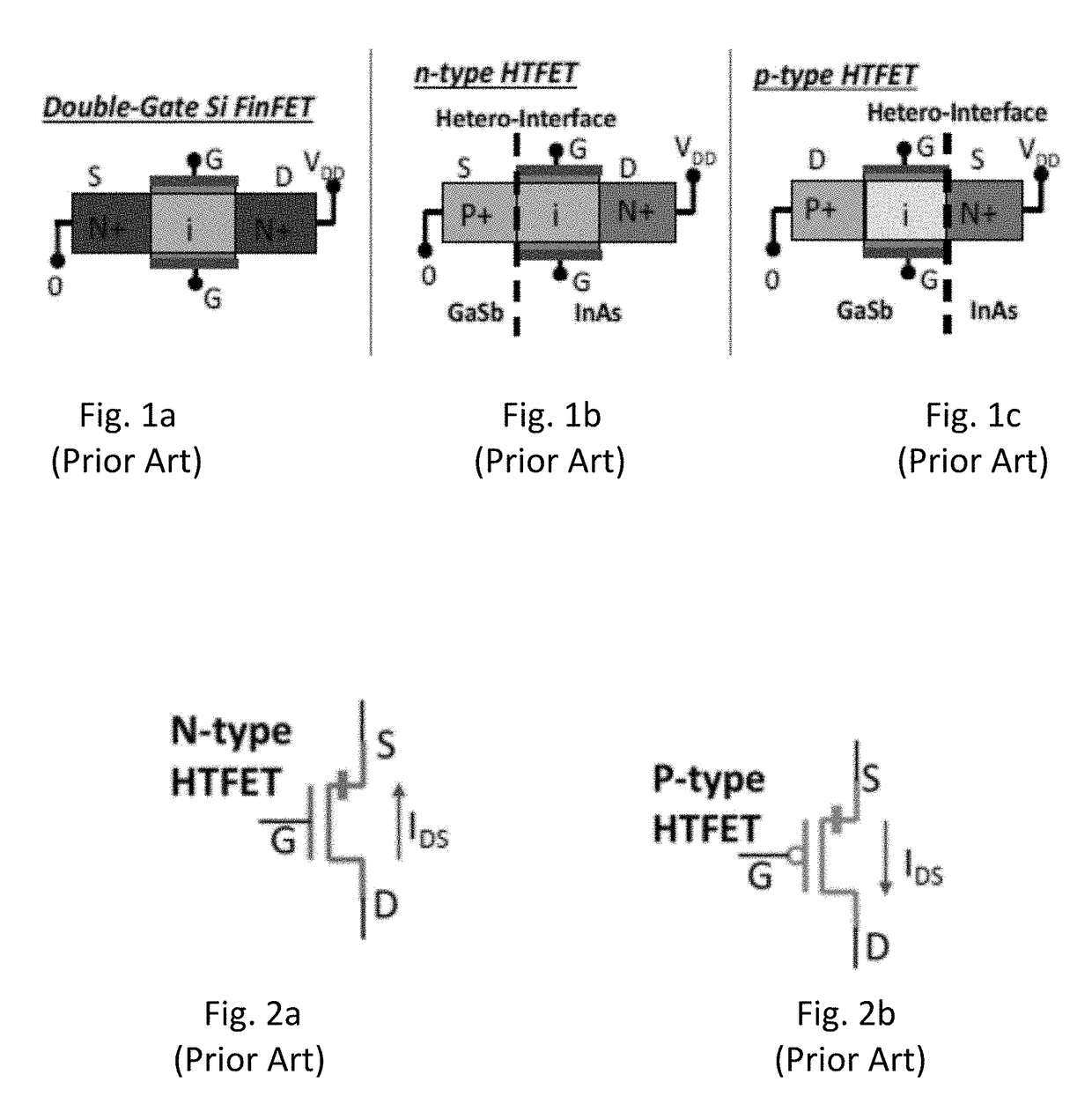
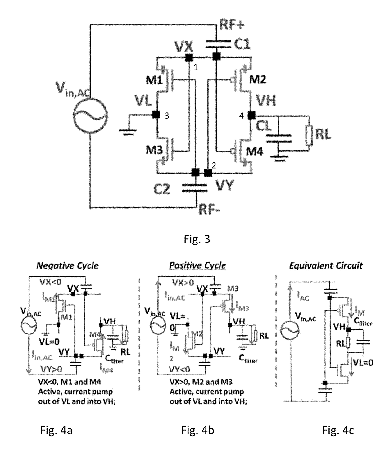
[0079]As shown in FIGS. 1b and 1c, a Tunneling Field Effect Transistor (“TFET”) can be seen as a reverse-biased, gated p-i-n tunnel diode with asymmetrical source / drain doping. The reverse biased diode leakage determines the current in the off-state, or Ioff, of the TFET. The on-state is enabled by the gate-controlled band-to-band tunneling at the source-channel junction, and a sub-60 mV / decade steep-slope can be achieved in TFET with desired Ion / Ioff over a low power supply, or VCC, range. Moreover, with the introduction of materials from group III and group V of the periodic table (III-V materials) and a heterojunction, a III-V Hetero-junction TFET (“HTFET”) exhibits improved energy efficiency for below 0.5V VCC compared to the state-of-art CMOS technology. As described herein, these advantages exhibited by the TFET may be used to generate RF-power system components that not only improve the functionalities of the components themselves, but also the functionalities of the RF-syste...


PUM


Abstract

Disclosed are low power electronic devices configured to exploit the sub-threshold swing, unidirectional tunneling, and low-voltage operation of steep slope-tunnel tunnel field-effect transistors (TFET) to improve power-conversion efficiency and power-efficiency of electrical systems incorporating the TFET as an electrical component to perform energy harvesting, signal processing, and related operations. The devices include a HTFET-based rectifier having various topologies, a HTFET-based DC-DC charge pump converter, a HTFET-based amplifier having an amplifier circuit including a telescopic operational transconductance amplifier, and a HTFET-based SAR A / D converter having a HTFET-based transmission gate DFF. Any one of the devices may be used to generate a RF-powered system with improved power conversion efficiencies of power harvesters and power efficiencies of processing components within the system.

Description

CROSS-REFERENCE TO RELATED APPLICATION[0001]This patent application claims the benefit of U.S. Provisional Patent Application No. 61 / 993,126, filed on May 14, 2014, which is hereby incorporated by reference in its entirety.STATEMENT REGARDING FEDERALLY SPONSORED RESEARCH OR DEVELOPMENT[0002]This invention was made with government support under Grant No. EEC1160483, awarded by the National Science Foundation and under Contract No. HR0011-13-3-0002, awarded by the Defense Advanced Research Projects Agency (DARPA). The Government has certain rights in the invention.FIELD OF THE INVENTION[0003]The present disclosure is generally directed towards low power electronics, and in particular energy harvesting and signal processing electronic components of RF-powered electronic systems that may operate with low input power.BACKGROUND OF THE INVENTION[0004]RF-power harvester circuits may be used to harvest ambient radio-frequency (“RF”) signals as a power source in RF-powered systems, such as p...

Claims


Application Information

Patent Timeline
Patent Type & Authority Patents(United States)
IPC IPC(8): H01F37/00H01L29/739H02J5/00H02J50/20H01F38/00
CPCH02J50/20H02J5/005H01L29/7391H02J50/001H02J5/00
Inventor LIU, HUICHUVADDI, RAMESHNARAYANAN, VIJAYKRISHNANDATTA, SUMANSEOK KIM, MOONLI, XUEQINGSCHMID, ALEXANDRESHOARAN, MAHSAHEO, UNSUK
Owner PENN STATE RES FOUND
Why Eureka
Try Eureka