Tapered vertical FET having III-V channel
- Summary
- Abstract
- Description
- Claims
- Application Information
AI Technical Summary
Benefits of technology
Problems solved by technology
Method used
Image

Examples
Embodiment Construction
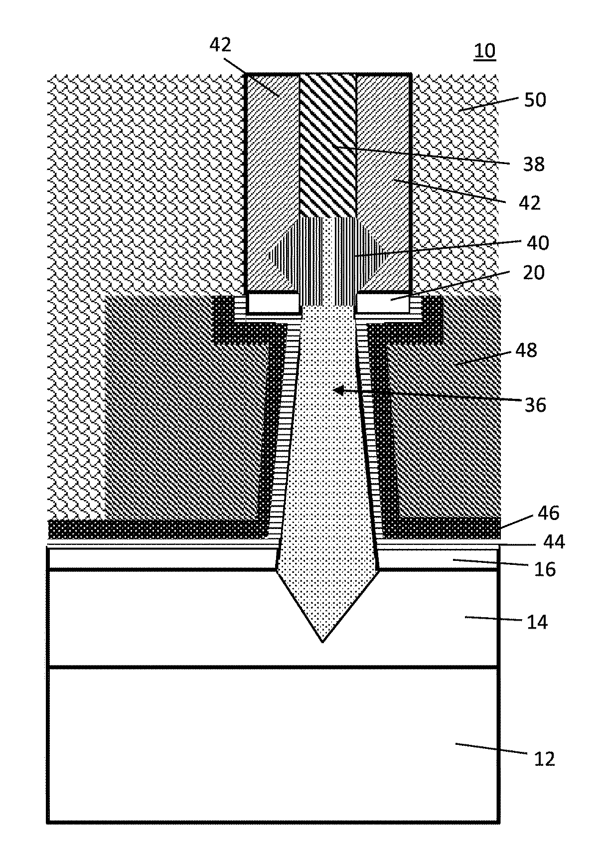
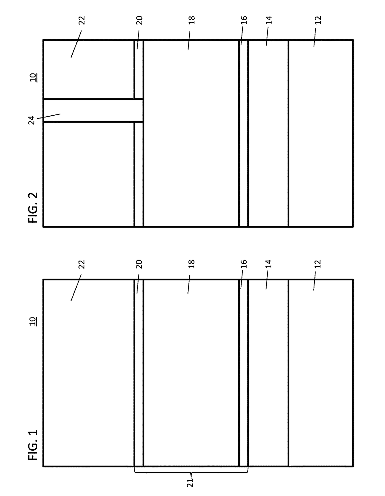
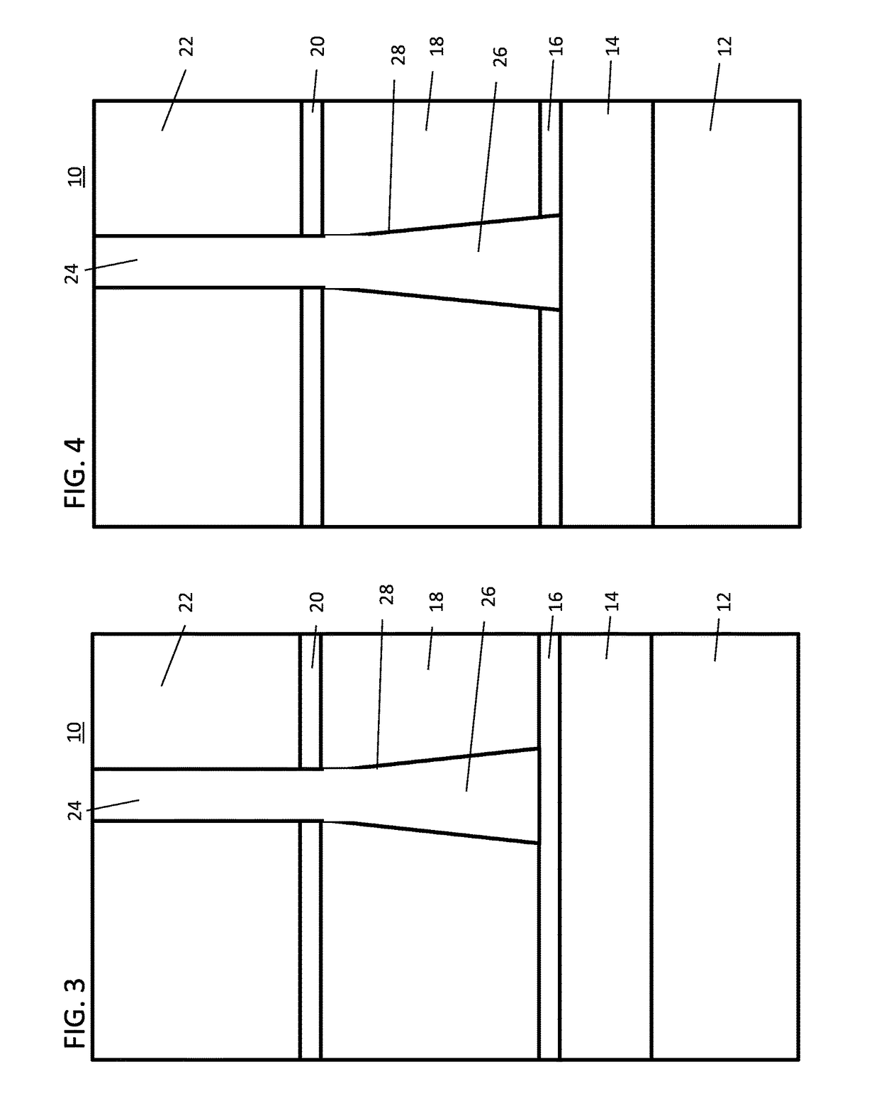
[0028]In accordance with the present principles, vertical transistors and methods for fabrication are provided. III-V channel materials are attractive due to their high electron mobility. However, the relatively narrow bandgap of such materials as compared to silicon results in high off-state leakage currents. In accordance with the present principles, vertical transistors include a tapered channel structure. In one embodiment, the channel structure includes a wide channel source, and a narrow channel drain. In other embodiments, this may be reversed. The tapered channel structure employs bandgap modulation by quantum confinement effects, which can occur at relatively wide channel widths (e.g., as large as 15 nm) for group III-V semiconductors. A wide bandgap drain reduces the leakage current caused by band-to-band tunneling.
[0029]In some embodiments, pass-gates may be fabricated using traditional non-tapered channels, and an optional anneal of source / drain regions may be performed ...
PUM
 Abstract
Description
Claims
Application Information
 - Generate Ideas
- Intellectual Property
- Life Sciences
- Materials
- Tech Scout
- Unparalleled Data Quality
- Higher Quality Content
- 60% Fewer Hallucinations
Browse by: Latest US Patents, China's latest patents, Technical Efficacy Thesaurus, Application Domain, Technology Topic, Popular Technical Reports.
© 2025 PatSnap. All rights reserved.Legal|Privacy policy|Modern Slavery Act Transparency Statement|Sitemap|About US| Contact US: help@patsnap.com