Static random access memory device and forming method thereof

a random access and memory device technology, applied in the direction of bulk negative resistance effect devices, transistors, instruments, etc., can solve the problems of high access speed and high cost, and achieve the effects of reducing soft error rate, reducing circuit leakage, and reducing reading interferen

Active Publication Date: 2018-01-16
UNITED MICROELECTRONICS CORP
View PDF15 Cites 3 Cited by
  • Summary
  • Abstract
  • Description
  • Claims
  • Application Information

AI Technical Summary

Benefits of technology

[0008]According to the above, the present invention provides a static random access memory device and forming method thereof, which has two resistive-switching devices, and two body contacts in a wafer electrically and respectively connecting the resistive-switching devices to a static random access memory cell, thereby reducing circuit leakage, decreasing the interference of reading and writing and reducing the soft error rate (SER).

Problems solved by technology

Static RAM is a complex structure, therefore having high access speed and high cost, thereby it is often used as a memory providing low capacity but high speed such as a 256 KB or 512 KB cache memory built-in a central processing unit (CPU) of a personal computer.

Method used


Image

  • Static random access memory device and forming method thereof
  • Static random access memory device and forming method thereof
  • Static random access memory device and forming method thereof

Examples


Embodiment Construction

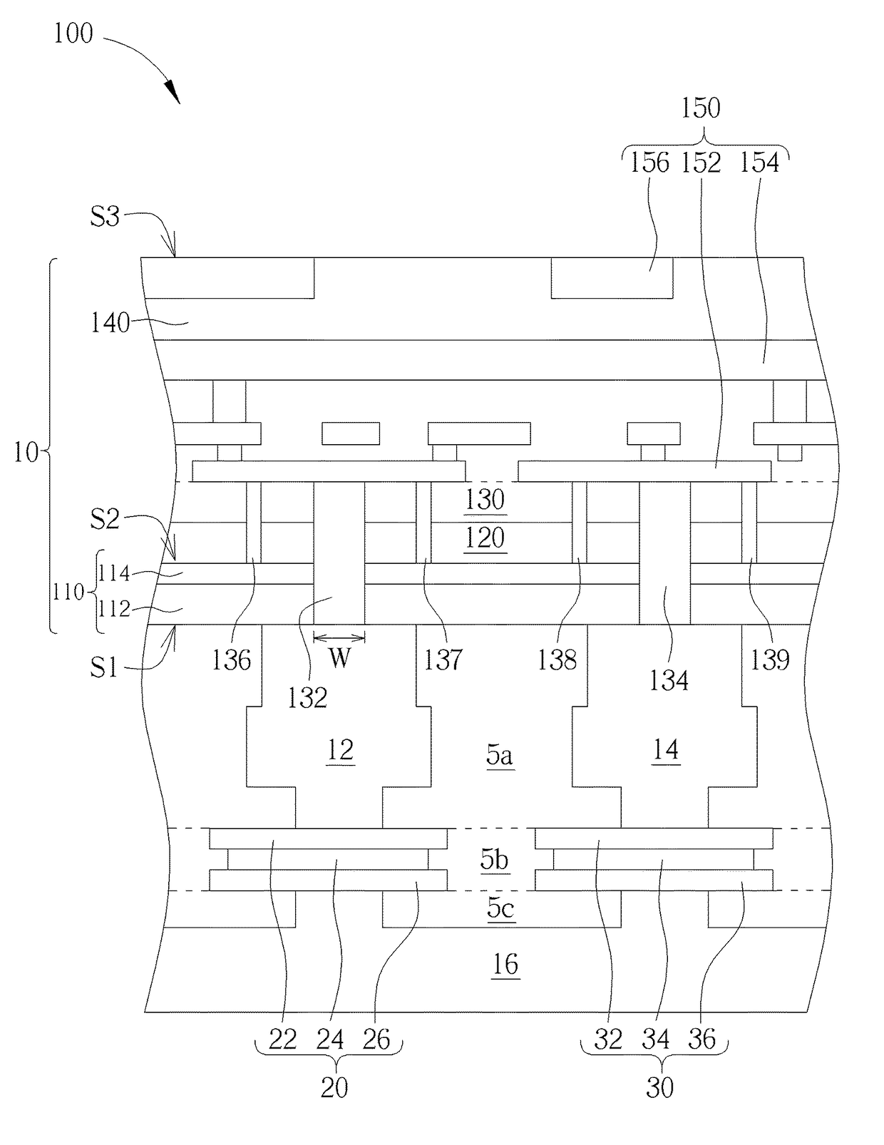
[0014]FIG. 1 schematically depicts a cross-sectional view of a static random access memory device according to an embodiment of the present invention. As shown in FIG. 1, a wafer 10 is provided. The wafer 10 includes a substrate 110, wherein the substrate 110 has a backside S1 and a front side S2. The substrate 110 may be a semiconductor substrate such as a silicon substrate, a silicon containing (such as silicon carbide) substrate, a III-V group-on-silicon (such as GaN-on-silicon) substrate, a graphene-on-silicon substrate, a silicon-on-insulator (SOI) substrate or a substrate containing epitaxial layers. In this embodiment, the substrate 110 is a silicon-on-insulator (SOI) substrate, thereby the substrate 110 has a bottom layer (not shown, which will be removed while the wafer 10 is reserved and thinned in later processes), an oxide layer 112 and a top layer 114 stacked from bottom to top. In this embodiment, the top layer 114 is a silicon layer, and the thickness of the top layer...


PUM


Abstract

A static random access memory device includes two body contacts and two resistive-switching devices. The body contacts are disposed in a wafer and are exposed from a back side of the wafer, wherein the body contacts electrically connect a static random access memory cell through a metal interconnect in the wafer. The resistive-switching devices connect the two body contacts respectively from the back side of the wafer. A method of forming a static random access memory device is also provided in the following. A wafer having two body contacts exposed from a back side of the wafer and a metal interconnect electrically connecting a static random access memory cell to the body contacts is provided. Two resistive-switching devices are formed to connect the two body contacts respectively from the back side of the wafer.

Description

BACKGROUND OF THE INVENTION1. Field of the Invention[0001]The present invention relates generally to a memory device and forming method thereof, and more specifically to a static random access memory device and forming method thereof.2. Description of the Prior Art[0002]Random access memory (RAM) can be operated to read data from it and write data into it. As computers containing RAM turn off, data disappears from the RAM immediately. Since data in RAM can be altered easily, RAM is widely used as temporary data storage memory in personal computers. RAM can be classified into dynamic-type and static-type.[0003]A dynamic random access memory (DRAM: Dynamic RAM) stores one-bit data by one transistor paired with one capacitor, and electricity must be supported during operating to keep this data, thus called Dynamic RAM. Dynamic RAM is a simple structure, therefore having slow access speed and low cost. Thus, it is often used as a memory providing high capacity but low speed such as a ma...

Claims


Application Information

Patent Timeline
Patent Type & Authority Patents(United States)
IPC IPC(8): H01L29/06H01L27/11H01L47/00H01L23/48G11C11/419G11C14/00H01L23/532H01L23/525H01L27/24H01L45/00
CPCH01L27/1116H01L27/1104H01L23/481H01L45/143H01L45/144H01L27/2463H01L23/525H01L23/532H01L45/1233H01L45/06G11C14/009G11C11/419H10B99/00H10B10/15H10B10/18H10B10/12H10B63/80H10N70/231H10N70/826H10N70/8825H10N70/8828
Inventor HE, WANXUNXING, SU
Owner UNITED MICROELECTRONICS CORP
Why Eureka
Try Eureka