Array of geiger-mode avalanche photodiodes for detecting infrared radiation

a geiger-mode avalanche and photodiode technology, applied in the field of geiger-mode avalanche photodiodes for detecting infrared radiation, can solve the problems of inability to detect photons, undesirable increase of dark current, and limited sensitive areas of arrays used in the context of infrared radiation detection

Active Publication Date: 2018-02-20
STMICROELECTRONICS SRL
View PDF6 Cites 27 Cited by
  • Summary
  • Abstract
  • Description
  • Claims
  • Application Information

AI Technical Summary

Problems solved by technology

Consequently, once the ionization process is triggered, the SPAD is no longer able to detect photons.
However, there further occurs, as mentioned previously, an undesirable increase in the dark current, which is triggered by spurious events such as optical crosstalk and afterpulsing.
Further, the arrays used in the context of detection of infrared radiation have limited sensitive areas (typically, in the region of a few square millimeters) since the dark current increases as the sensitive area increases.

Method used


Image

  • Array of geiger-mode avalanche photodiodes for detecting infrared radiation
  • Array of geiger-mode avalanche photodiodes for detecting infrared radiation
  • Array of geiger-mode avalanche photodiodes for detecting infrared radiation

Examples


Embodiment Construction

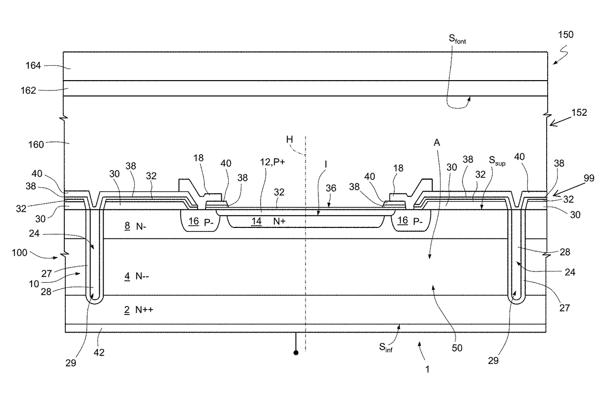
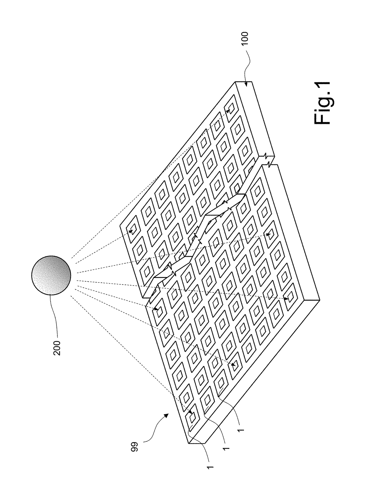
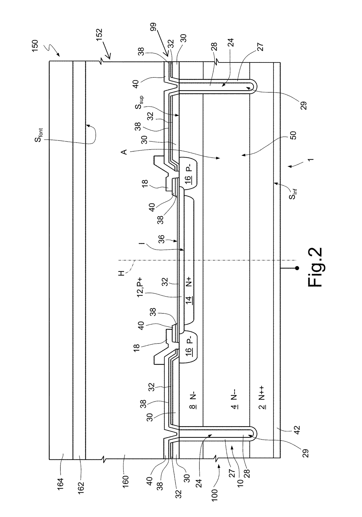
[0023]FIG. 1 shows an embodiment of an array 99 of SPADs 1, which are arranged in planar fashion and are illuminated by a light source 200. The array 99 may comprise any number of SPADs 1, according to the need. Further, the array 99 is integrated in a die 100, which, as shown in FIG. 2 (which is not in scale), comprises a semiconductor body 10 made, for example, of silicon.

[0024]Purely by way of example, the semiconductor body 10 comprises a substrate 2, which is delimited at the bottom and at the top by a bottom surface Sinf and a top surface Ssup, respectively. Further, the semiconductor body 10 comprises a first epitaxial layer 4 and a second epitaxial layer 8.

[0025]The substrate 2 is of an N++ type, has a thickness, for example, of between 300 μm and 500 μm and has a doping level, for example, of between 1·1019 cm−3 and 5·1020 cm−3. Further, the substrate 2 forms the aforementioned bottom surface Sinf.

[0026]The first epitaxial layer 4 is of an N−− type, has a thickness, for exa...


PUM


Abstract

An array of Geiger-mode avalanche photodiodes is formed in a die and includes: an internal dielectric structure, arranged on the die; and an external dielectric region arranged on the internal dielectric structure. The external dielectric region is formed by an external material that absorbs radiation having a wavelength that falls in a stop-band with low wavelength and transmits radiation having a wavelength that falls in a pass-band with high wavelength, at least part of the pass-band including wavelengths in the infrared. The internal dielectric structure is formed by one or more internal materials that substantially transmit radiation having a wavelength that falls in the stop-band and in the pass-band and have refractive indices that fall in an interval having an amplitude of 0.4. In the stop-band and in the pass-band the external dielectric region has a refractive index with the real part that falls in the above interval.

Description

BACKGROUNDTechnical Field[0001]The present disclosure relates to an array of Geiger-mode photodiodes for detecting infrared radiation.Description of the Related Art[0002]As is known, today sensors for detecting infrared radiation (i.e., radiation with a wavelength of between 700 nm and 2000 nm) find widespread use not only in the sector of telecommunications, but also, for example, in the sector of so-called 3D imaging, as well as, once again by way of example, in the sector of thermography and plethysmography.[0003]Currently used for detection of infrared radiation are, among other things, semiconductor sensors operating in the linear region, avalanche photodetectors, phototransistors, and vacuum photomultiplier tubes. Instead, the so-called arrays of Geiger-mode avalanche photodiodes (GMAPs) are relatively little used in the field of detection of infrared radiation, since, even though they guarantee a good sensitivity in regard to infrared radiation, they are subject to dark curre...

Claims


Application Information

Patent Timeline
Patent Type & Authority Patents(United States)
IPC IPC(8): H01L31/07H01L31/02H01L31/0216H01L27/144H01L31/107G01J1/44
CPCH01L31/02164G01J1/44H01L31/02027H01L31/107H01L27/1446G01J2001/4466H01L25/0753H01L33/54H01L33/58H01L27/1462H01L27/14625H01L27/1463H01L27/14649
Inventor MAZZILLO, MASSIMO CATALDOFALLICA, PIEROLOMBARDO, SALVATORE
Owner STMICROELECTRONICS SRL
Why Eureka
Try Eureka