Spacer and manufacturing device for the same

a technology of spacer and liquid crystal panel, which is applied in the direction of microlithography exposure apparatus, instruments, photomechanical treatment, etc., can solve the problems of poor light transmission effect, poor and the adverse impact of the display effect, etc., to achieve low manufacturing cost, simple process, and increase density and width of the sub-light transmitting region

Active Publication Date: 2018-04-17
TCL CHINA STAR OPTOELECTRONICS TECH CO LTD
View PDF12 Cites 2 Cited by
  • Summary
  • Abstract
  • Description
  • Claims
  • Application Information

AI Technical Summary

Benefits of technology

[0007]In order to overcome the drawbacks of the conventional art, the present invention provides a spacer and a manufacturing device for the same, which has a high pixel aperture ratio and an easy manufacturing process.
[0019]The spacer manufacturing device of the present invention disposes a central light-transmitting region and a peripheral light-transmitting region which having different light intensity on a same photo mask such that after the lights emitted from the exposure device irradiates on the negative photoresist material, the light intensity at a center and the light intensity at a periphery are different so that a height of a spacer formed at the center region is greater than a height of a spacer formed at the periphery region. Accordingly, only one exposure process is required to realize the spacer having a convex-shaped cross section. The process is simple and the manufacturing cost is low. At the same time, the manufacturing device also includes multiple photo masks. A shape and a size of the peripheral light-transmitting region of each photo mask are different. Besides, a density and a width of the sub-light-transmitting regions can be increased or the irradiation parameters of the exposure device can be regulated to adjust a uniformity of the peripheral light-transmitting region of the photo mask. Finally, a flatness of the convex shoulder of the spacer having a convex-shaped cross section is adjustable, which can satisfy the requirement for manufacturing spacers having different specifications.

Problems solved by technology

Besides, the liquid crystal product usually suffers an external force impact such as a touch so that a misalignment of the substrates of the liquid crystal display panel is easily generated so as to cause a light leakage problem of the panel.
Accordingly, adverse impacts of the display effect such as wrong display colors or bad display effect is generated.
Similarly, two exposure processes are required so that the manufacturing cost is still high.

Method used


Image

  • Spacer and manufacturing device for the same
  • Spacer and manufacturing device for the same
  • Spacer and manufacturing device for the same

Examples


Embodiment Construction

[0031]The following content combines with the drawings and the embodiment for describing the present invention in detail. It is obvious that the following embodiments are only some embodiments of the present invention. For the person of ordinary skill in the art without creative effort, the other embodiments obtained thereby are still covered by the present invention.

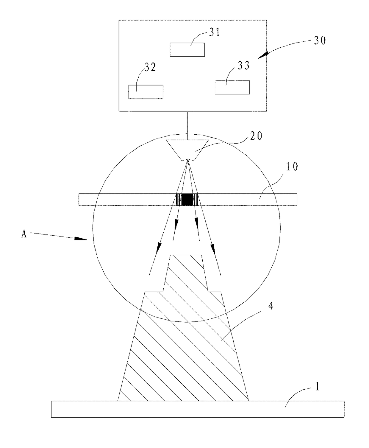
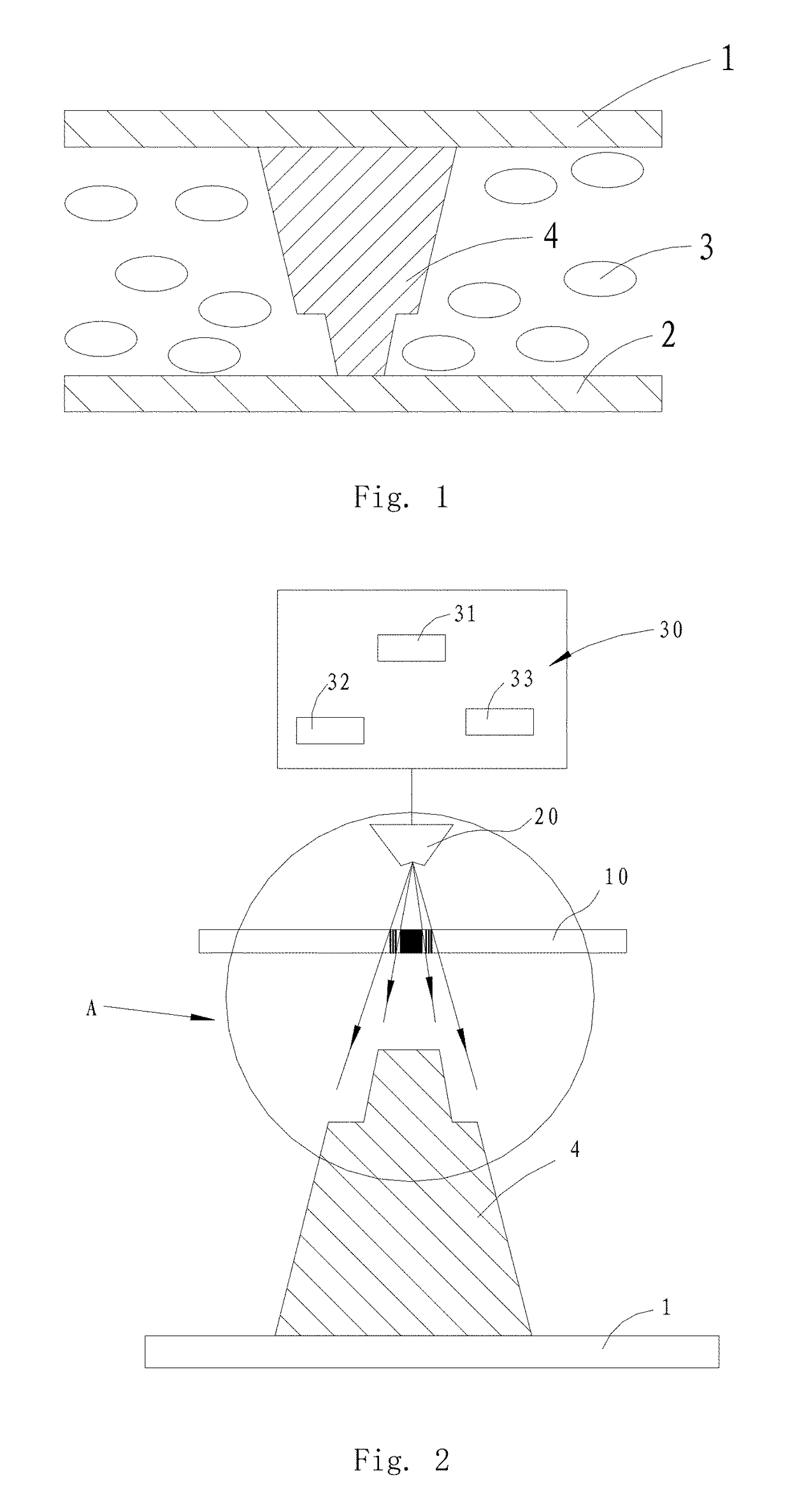
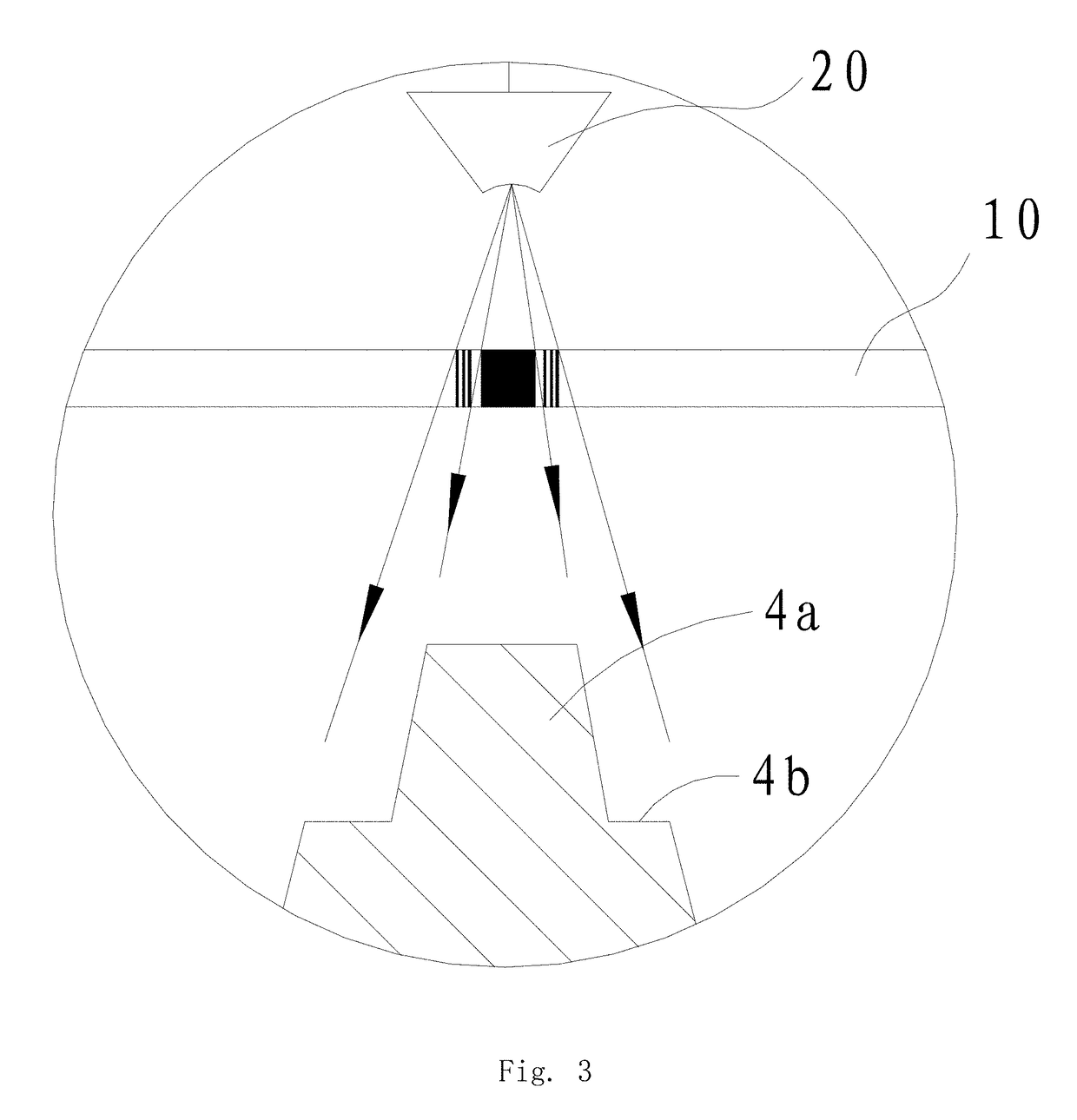
[0032]With reference to FIG. 1, the display panel of the present invention includes an upper color filter substrate 1, a lower array substrate 2, and liquid crystal molecules filled between the color filter substrate 1 and the array substrate 2. At the same time, a spacer 4 having a convex-shaped cross section is located between the color filter substrate 1 and the array substrate 2, and supports the color filter substrate 1 and the array substrate 2. Besides, the spacer 4 having a convex-shaped cross section has both functions of a main post spacer (PS) and a sub post spacer (PS). The spacer 4 having a convex-shaped cr...


PUM

PropertyMeasurementUnit
light intensityaaaaaaaaaa
widthsaaaaaaaaaa
exposure distanceaaaaaaaaaa

Abstract

A spacer manufacturing device is disclosed. The device includes a photo mask having a central light-transmitting region and a peripheral light-transmitting region disposed at a periphery of the central light-transmitting region; and an exposure device right opposite to the photo mask. Wherein, light emitted from the exposure device is irradiated to a negative photoresist material after passing through the photo mask, the light intensity passing through the peripheral light-transmitting region is less than the light intensity passing through the central light-transmitting region. A spacer is also disclosed. Only one exposure process is required to realize the spacer having a convex-shaped cross section. The process is simple and the manufacturing cost is low. At the same time, a flatness of the convex shoulder of the spacer having a convex-shaped cross section is adjustable, which can satisfy the requirement for manufacturing spacers having different specifications.

Description

BACKGROUND OF THE INVENTION[0001]1. Field of the Invention[0002]The present invention relates to a spacer for a liquid crystal panel, and more particularly to a spacer and a manufacturing device for the same.[0003]2. Description of Related Art[0004]With the development of the display technology, a liquid crystal panel is widely applied. However, the liquid crystal panel is formed by injecting liquid crystal molecules between an array substrate and a color filter substrate. The structure of the liquid crystal panel decides that when an external temperature is changed, a material expansion or a material shrinkage of the glass substrate and the liquid crystal molecules. Besides, the liquid crystal product usually suffers an external force impact such as a touch so that a misalignment of the substrates of the liquid crystal display panel is easily generated so as to cause a light leakage problem of the panel. Accordingly, adverse impacts of the display effect such as wrong display color...

Claims


Application Information

Patent Timeline
Patent Type & Authority Patents(United States)
IPC IPC(8): G03F1/70G03F7/20G03F7/00G03F1/36G03F1/78G02F1/1339
CPCG03F1/70G03F1/36G03F7/0005G03F7/70283G03F1/78G02F1/13394G03F7/0007G02F1/13398
Inventor LIU, HUANWANG, ZUIGUO, JINBOLO, SHIH-HSUN
Owner TCL CHINA STAR OPTOELECTRONICS TECH CO LTD
Why Eureka
Try Eureka