Debugging in a semiconductor device test environment

a test environment and semiconductor technology, applied in the field of electronic system testing, can solve the problems of reducing affecting the quality affecting the accuracy of the test program, so as to reduce the time to debug a dut and/or a test program.

Active Publication Date: 2018-05-01
TERADYNE
View PDF47 Cites 7 Cited by
  • Summary
  • Abstract
  • Description
  • Claims
  • Application Information

AI Technical Summary

Benefits of technology

[0013]Such an interface may translate commands, derived based on the test program and the debug commands, into high level commands that may be processed by the test system. Processing by the test system may ultimately generate a test pattern and other instrument control signals on the fly. By using the debug system, a user may perform multiple operations without rewriting and reloading a test program. As a result, time to debug a DUT and / or a test program may be reduced

Problems solved by technology

If such tests indicate that the device is not working properly, the device is often diverted such that different operations to rework or scrap the device are performed.
These test programs are designed to exercise portions of the DUT, and are often written to surface design flaws in the DUT.
Test programs created for this purpose may be limited to testing small portions of the DUT at a time.
Though, changes to the test program may also result.
These iterations can be compounded if, during testing, a problem with the design of the DUT is identified, requiring changes to the design.
For example, if multiple devices that have been manufactured and put into use are experience similar defects, a manufacturer of the device may want to test samples to determine whether the failures are related to a latent defect in the design or systemic defects in the manufacture of the devices.

Method used


Image

  • Debugging in a semiconductor device test environment
  • Debugging in a semiconductor device test environment
  • Debugging in a semiconductor device test environment

Examples


Embodiment Construction

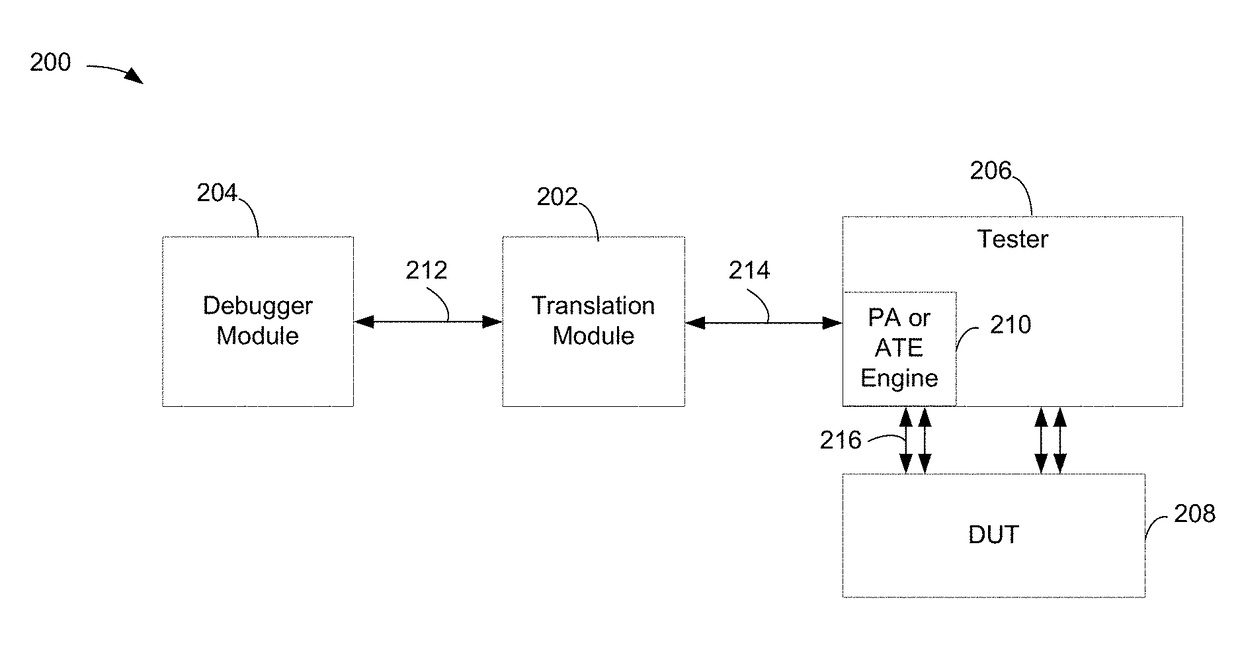
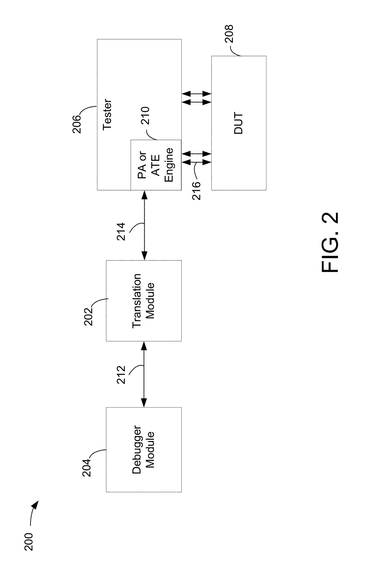
[0026]Using techniques described herein, a test system may be adapted to provide real-time, interactive debugging of a device under test (DUT). The system may leverage investment in a tester that a semiconductor device manufacturer might otherwise acquire for manufacturing testing of engineering work. Yet, such the tester may be used in a way that speeds semiconductor devices to market or facilitates identification and correction of design or systemic manufacturing defects of devices in comparison to conventional use of a tester.

[0027]In accordance with some embodiments, a customer may provide a test program, containing multiple test program commands. A debugger may, in response to debug inputs provided by a user, generate debug commands. These debug commands may be based on the test program commands, for example by indicating that test program commands should be executed at times or in ways determined by the debug inputs. Such debug commands may include stepping through the test pr...


PUM


Abstract

A test system that enables real-time interactive debugging of a device under test (DUT) using native customer code. A translation module may format, in real time, debug commands, corresponding to a user input, into a format recognizable by instruments in a tester. The user input may be a test program or test instructions written in a high-level programming language. The translation module may translate the user's debug commands into lower-level test instrument commands, based on which the tester may apply control signals to a processor in the DUT to test subsystems of the DUT. A result of the test may be provided to the translation module, which may, in real time, format another debug command, or provide an indication of the result to the user. The translation module may thus enable a user to step-through and modify native customer code in an interactive manner to debug a DUT.

Description

BACKGROUND[0001]1. Field of the Invention[0002]The invention relates generally to testing of electronic systems, such as system-on-chip semiconductor devices.[0003]2. Related Art[0004]Automatic test equipment (referred to generally as a “tester”) is known for testing many types of electronic devices under test (DUTs). For example, testers for test printed circuit boards and semiconductor devices are known.[0005]In some scenarios, testers are used during manufacture of the electronic devices. In this capacity, the testers are used to identify defects such that the results of testing can be used to impact the manufacture of a DUT by conditioning certain operations on the results of testing. For example, manufacturing steps that result in the device being packaged and shipped to a customer are typically performed only if testing on a device indicates that the device is working properly. If such tests indicate that the device is not working properly, the device is often diverted such th...

Claims


Application Information

Patent Timeline
Patent Type & Authority Patents(United States)
IPC IPC(8): G06F11/36G06F11/263G01R31/317G01R31/319G06F11/273G06F11/22
CPCG06F11/2733G01R31/319G01R31/31705G06F11/362G06F11/2294G06F11/263G01R31/31707
Inventor HUTNER, MARC REUBENROWE, JOHN F.
Owner TERADYNE
Why Eureka
Try Eureka