Data processor and data processing system and method for accessing a dynamic type memory using an address multiplexing system

a data processor and data processing system technology, applied in the field of data processing technology, can solve the problems of large packaging area of the system, more troublesome control of the system than that of the rom, and inability to design the system, and achieve the effect of high versatility

Inactive Publication Date: 2000-01-04
HITACHI LTD
View PDF10 Cites 2 Cited by
  • Summary
  • Abstract
  • Description
  • Claims
  • Application Information

AI Technical Summary

Benefits of technology

A microprocessor comprises therein a refresh counter which generates a refresh address, a control signal forming circuit which forms control signals, such as RAS signal and CAS signal, required for accessing a dynamic RAM, and a register which designates either access to the dynamic RAM or access to a static RAM (or a ROM), an address outputting mode being alterable in accordance with the content of the register, whereby not only the static RAM but also the dynamic RAM can be accessed, and the latter can be refreshed without disposing any external circuit, to facilitate the design of a system and to reduce the packaging area of the system.
In addition, the above register comprises registers which designate the address ranges and capacities of the dynamic RAMs to be used, namely, the number of bits of address signals, thereby to provide a microprocessor of high versatility in which the capacities or number of the dynamic RAMs to be used can be changed freely to some extent.

Problems solved by technology

Since, however, the dynamic RAM requires an address multiplexing system and requires a refresh operation, the control thereof is more troublesome than those of the ROM and the static RAM.
In this manner, the use of the dynamic RAM for the prior-art microprocessor has led to the problems that the design of the system becomes difficult and that the packaging area of the system becomes large.

Method used


Image

  • Data processor and data processing system and method for accessing a dynamic type memory using an address multiplexing system
  • Data processor and data processing system and method for accessing a dynamic type memory using an address multiplexing system
  • Data processor and data processing system and method for accessing a dynamic type memory using an address multiplexing system

Examples


embodiment 1

[Embodiment 1]

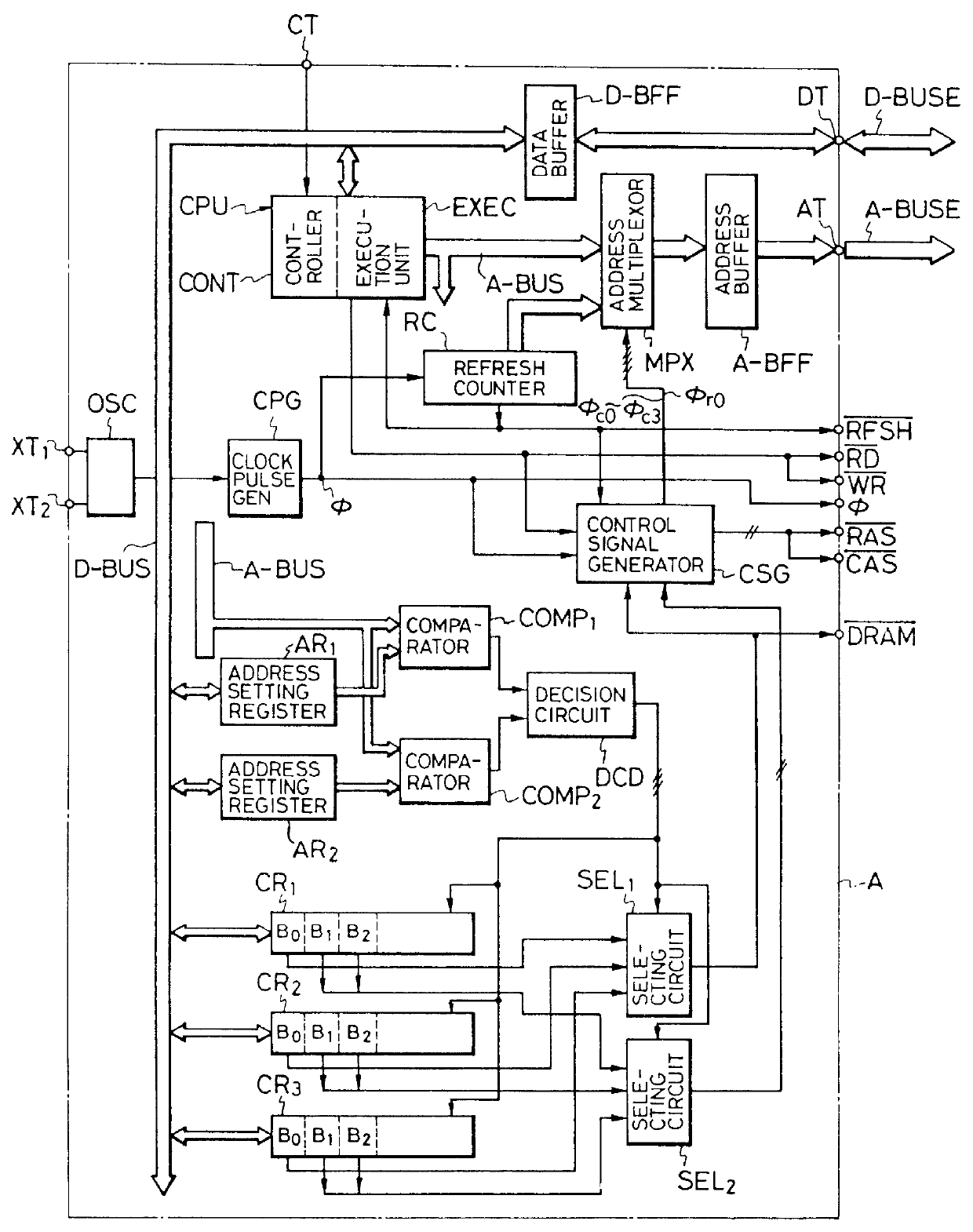
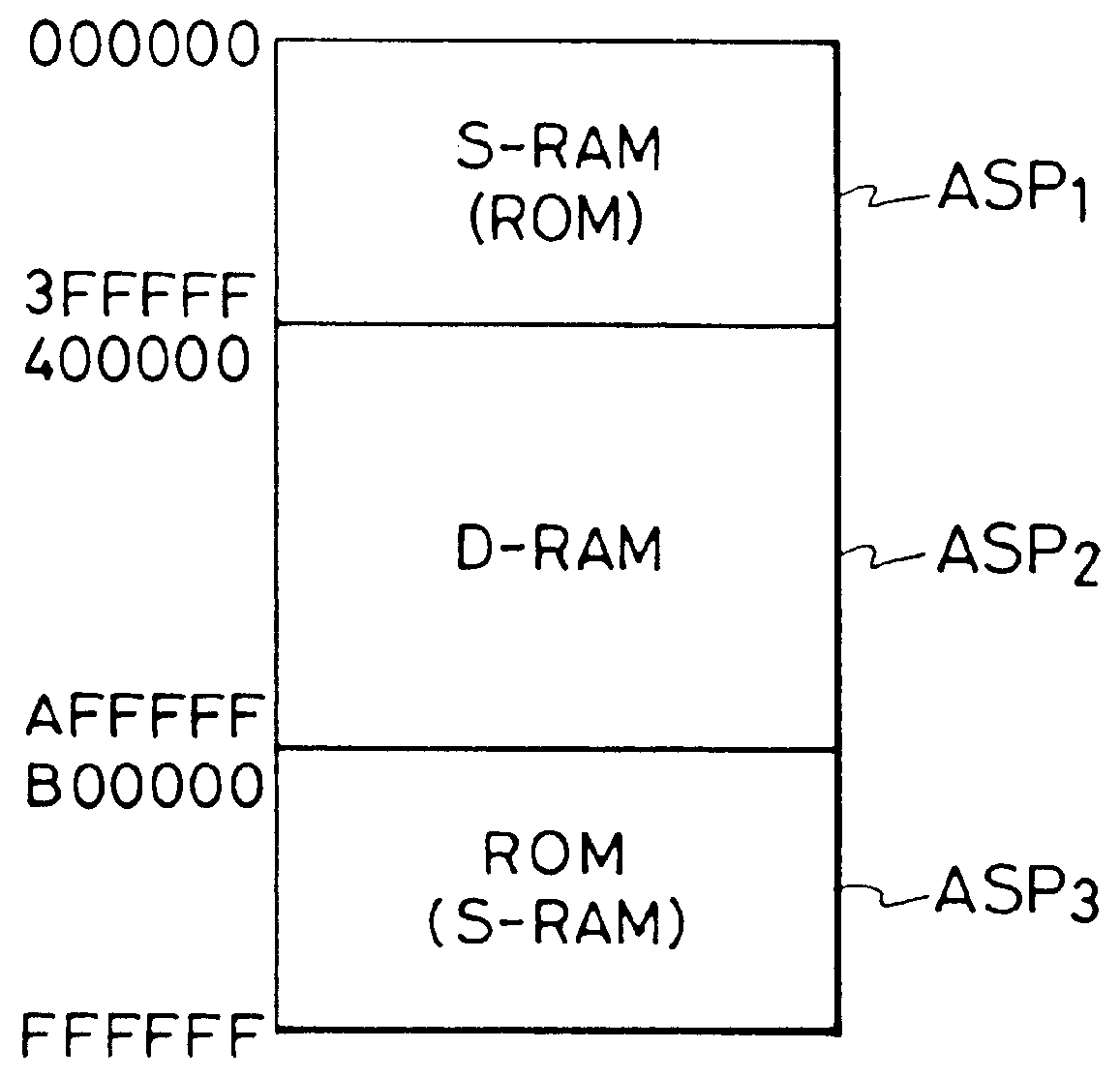
FIG. 1 is a circuit block diagram of one embodiment in the case of applying the present invention to a 16-bit microprocessor. In the figure, a portion enclosed with a chain line A is formed on a single semiconductor substrate such as single-crystal silicon by known semiconductor production technology.

In FIG. 1, shown by circuit symbol CPU is a microprocessor portion. Although this microprocessor portion CPU, the practicable arrangement of which is not directly pertinent to the present invention, is not illustrated in detail, it is constructed of for example execution unit EXEC which is composed of an arithmetic-logic unit, dedicated registers such as a program counter, a stack pointer, a status register, and general-purpose registers for use as work areas, and a controller CONT which is composed of an instruction register to which microprogram instructions read out from an external memory not shown are successively input. micro ROMs in which microinstructions correspon...

embodiment 2

[Embodiment 2]

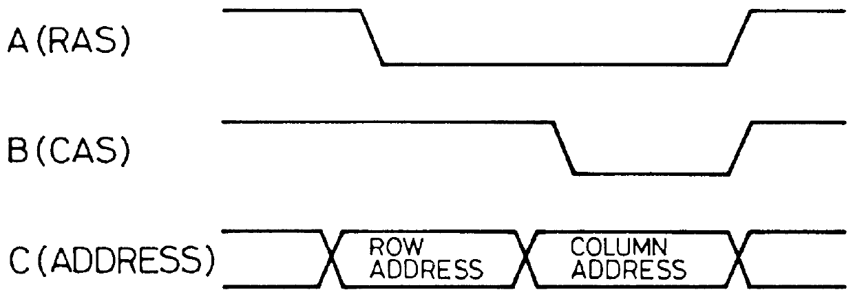
FIG. 13 is a circuit diagram of an address multiplexor MPX and a part of a control signal generator CSG in another embodiment.

In this embodiment, timing signals .phi..sub.r0, .phi..sub.c0 and .phi..sub.ref in the control signal generator CSG are respectively the same as those of the preceding embodiment.

In the control signal generator CSG, an inverter circuit IV.sub.45 and an AND gate circuit G.sub.1 constitute a decoder which forms an output signal of high level when bit signals B.sub.1 and B.sub.2 are "1" and "0" respectively, namely, when the bit signals B.sub.1 and B.sub.2 indicates a memory such as 64-kilobit memory of 1-bit format.

A timing signal .phi..sub.r1 to be output from an OR gate circuit G.sub.2 is brought to the high level in synchronism with the timing signal .phi..sub.r0 if the bit signals B.sub.1 and B.sub.2 indicate the 64-kilobit memory, and it is maintained at the high level irrespective of the timing signal .phi..sub.r0 unless the bit signals B.su...


PUM


Abstract

A microprocessor has a register in which attributive data corresponding to a memory to be coupled to the microprocessor is written, and a control circuit which controls address signals to be supplied to the memory in accordance with the attributive data. The attributive data is composed of range data for discriminating ranges of address data supplied to an address bus, system data indicative of addressing systems of the memories corresponding to the respective address ranges, and bit number data indicative of numbers of address bits of the memories. Thus, in a case where the memory to be accessed is of an address multiplexing system as in a dynamic RAM, the address data of the address bus is divided into row address data and column address data, which are then supplied to the memory in time division.

Description

BACKGROUND OF THE INVENTIONThis invention relates to data processing technology, and more particularly to technology which is especially effective when applied to a microprocessor.A microcomputer system is constructed of a microprocessor, storage devices such as a ROM (read-only memory) and a RAM (random access memory), an input / output interface (I / O), etc. In this case;, the use of a dynamic RAM is better than the use of a static RAM because of the merit that the system can be arranged less expensively.Since, however, the dynamic RAM requires an address multiplexing system and requires a refresh operation, the control thereof is more troublesome than those of the ROM and the static RAM. Therefore, any of prior-art microprocessors has been constructed so as to be capable of direct access to the ROM and the static RAM. When arranging the system to use a dynamic RAM, it has been necessary to dispose complicated external circuits including circuits for forming RAS (row address strobe) ...

Claims


Application Information

Patent Timeline
Patent Type & Authority Patents(United States)
IPC IPC(8): G06F12/06G06F12/00G11C11/406G06F12/02G06F15/78
CPCG06F12/0653G06F12/00
Inventor BABA, SHIRO
Owner HITACHI LTD
Why Eureka
Try Eureka