Semiconductor laser with integral spatial mode filter

a technology of spatial mode filter and semiconductor laser, which is applied in the field of external cavity semiconductor lasers, can solve the problems of mw cw, associated higher output power, and generally low output power, and achieve the effect of high power amplification of forward propagating ligh

Inactive Publication Date: 2001-09-04
JDS UNIPHASE CORP
View PDF30 Cites 24 Cited by
  • Summary
  • Abstract
  • Description
  • Claims
  • Application Information

AI Technical Summary

Benefits of technology

The above objects are met with a laser in which a semiconductor active medium is located within an at most marginally stable resonant cavity with a single-spatial-mode filter therein. The semiconductor active medium is preferably an electrically pumped light amplifying diode heterostructure or "amplifier chip" that has a flared gain region with a narrow, single mode, optical aperture end and a broad light output end. The flared gain region permits the light to freely diffract as it propagates in the gain region, so the light has a diverging phase front. Only the central-most light rays of backward propagating light can pass through the narrow aperture end of the flared gain region to reach an external rear reflector of the resonant cavity. Rear reflectors integral with the diode heterostructure could also be used. The rear reflector can be a mirror surface or a frequency selective grating reflector. Orientation of the grating reflector determines which wavelength of light will couple back through the narrow aperture in the amplifier chip into the flared gain region. The flared gain region ensures high power amplification of forward propagating light while maintaining a single spatial mode of oscillation.

Problems solved by technology

A problem with previously available external-cavity semiconductor lasers is their generally low output power (on the order of 10 mW cw and 200-300 mW pulsed).
Further, higher output powers are associated with unstable output intensity and frequency and less than good modal quality.

Method used


Image

  • Semiconductor laser with integral spatial mode filter
  • Semiconductor laser with integral spatial mode filter
  • Semiconductor laser with integral spatial mode filter

Examples


Embodiment Construction

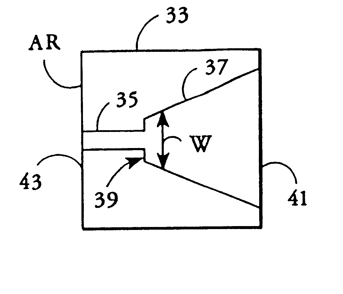
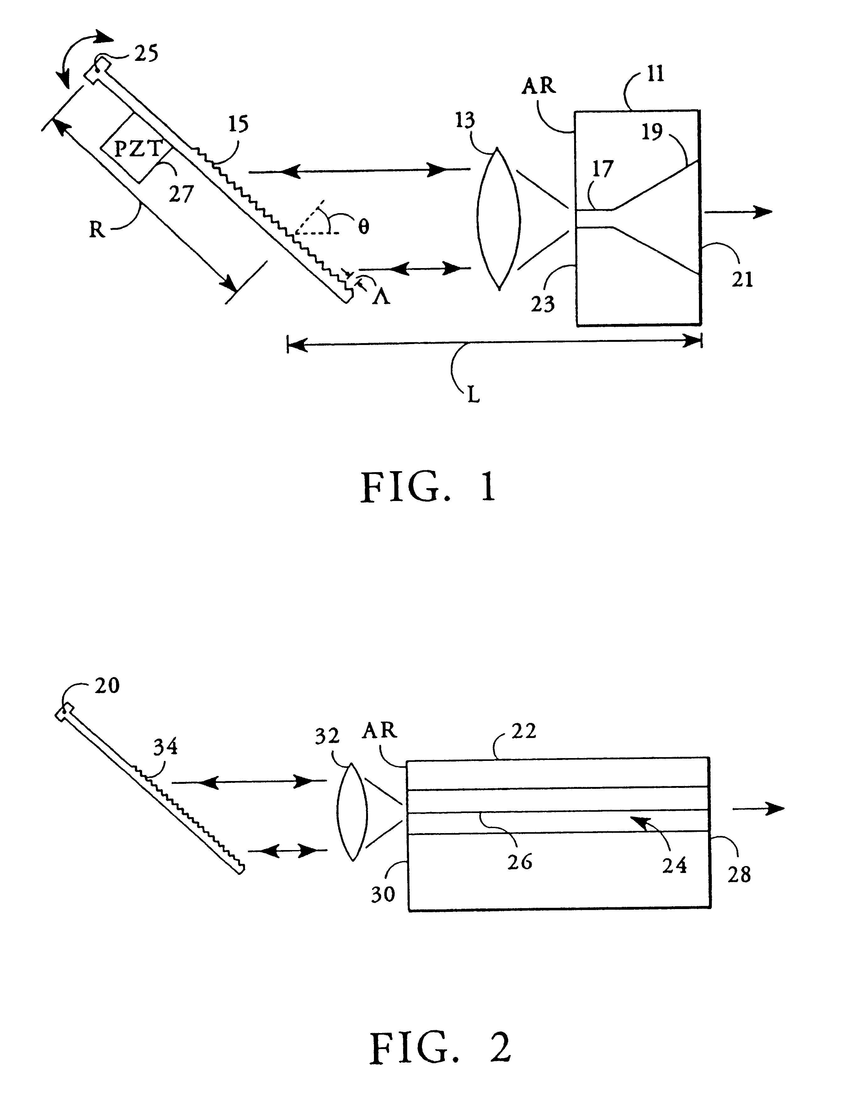
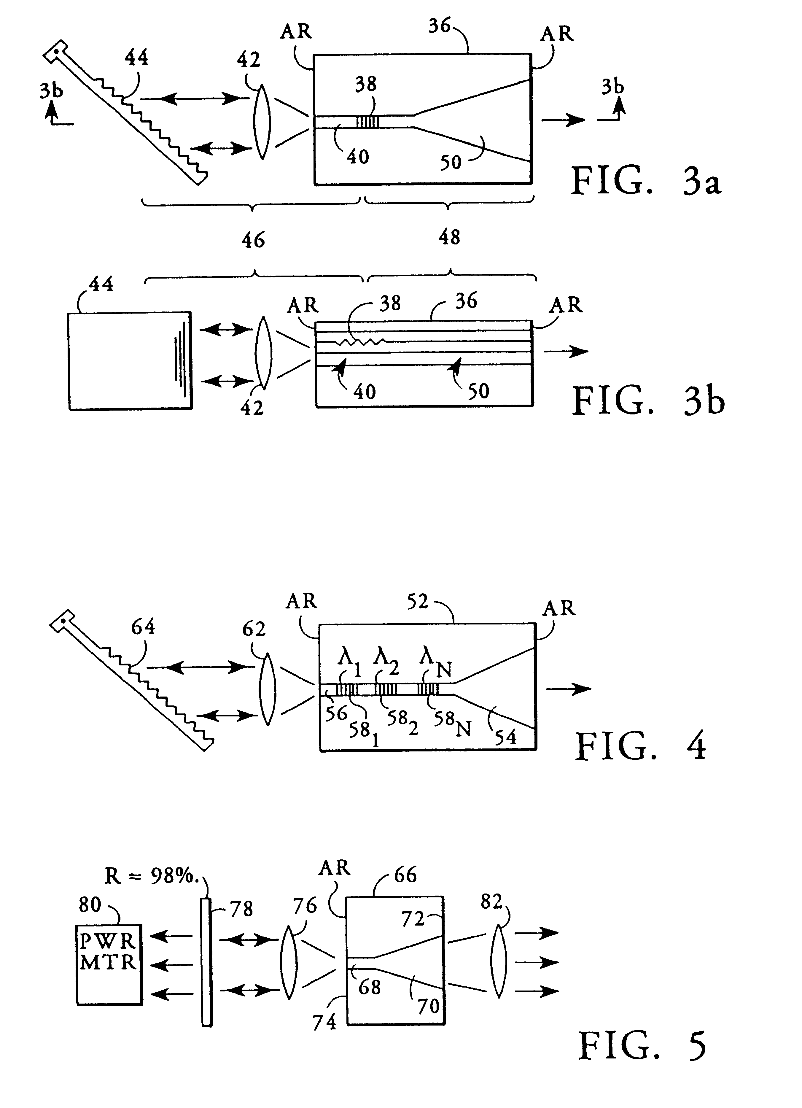
With reference to FIG. 1, an external-cavity semiconductor laser, in accord with one embodiment of the present invention, has an active gain medium that is a light amplifying diode heterostructure or "amplifier chip" 11, and also has a light reflective, external, diffraction grating 15 and a lens 13. The amplifier chip 11 shown in FIG. 1 has a single mode waveguide section 17 incorporated on the grating side of the chip, opening into a flared gain section 19 on the output side of the chip. Preferably, the flared gain region 19 is linearly flared and increases in width toward the front output facet 21 of the amplifier chip 11 at a rate that is slightly greater than the divergence of light propagating within the flared gain region 19. The front output facet 21 is typically coated for low reflection. Though a facet reflectivity of 30% would likely be acceptable, typically the reflectivity of the coated facet 21 is less than 10%, with a 2 to 3% reflectivity being preferred. The rear fac...


PUM


Abstract

A semiconductor laser having a light amplifying diode heterostructure with a flared gain region in an external resonant cavity. The flared gain region has a narrow aperture end which may be coupled to a single mode waveguide and a wide output end. A light emitting surface of the heterostructure proximate to the wide end of the flared gain region is partially reflective and combines with an external reflector to form a resonant cavity that is effectively unstable. The intracavity light-emitting surface proximate to the narrow aperture end is antireflection coated. The external reflector may be a planar mirror or a grating reflector. A lens or an optical fiber may couple the aperture end of the flared gain region to the external reflector. Frequency-selective feedback is provided by orienting the grating reflector or providing a prism in the cavity in front of the external planar mirror. Other filtering elements may also be placed in the external cavity. The flared gain region and waveguide may be differentially pumped or modulated with current provided by separate contacts.

Description

TECHNICAL FIELDThe present invention relates to external-cavity semiconductor lasers, especially to those laser that include a frequency-selective tuning element for broadband tunability and narrow linewidth light emission. The invention also relates to lasers with single spatial mode, diffraction-limited emission, and to light amplifying diode heterostructures with flared gain regions.BACKGROUND ARTExternal-cavity semiconductor lasers, including lasers with frequency selective tuning elements in the cavity, are well known and have been extensively studied. For example, T. Fujita, et al., in Applied Physics Letters 51(6), pages 392-394 (1987), describe a laser having a buried heterostructure laser that has been antireflection (AR) coated on the intracavity facet, a collimating lens, a polarization beamsplitter, external cavity mirrors in each of the TE and TM polarization light paths, and an electro-optic modulator in the TE polarization path between the beamsplitter and cavity mirr...

Claims


Application Information

Patent Timeline
Patent Type & Authority Patents(United States)
IPC IPC(8): H01S5/20H01S5/026H01S5/065H01S5/10H01S5/00H01S5/14H01S3/081H01S5/40H01S5/50H01S3/23H01S5/042H01S5/18H01S5/187H01S5/0625H01S5/125H01S5/12H01S5/185
CPCG02B6/12004G02B6/305H01S3/0818H01S3/113H01S5/026H01S5/0286H01S5/0625H01S5/06256H01S5/0655H01S5/1003H01S5/1014H01S5/1064H01S5/1082H01S5/1085H01S5/1215H01S5/125H01S5/14H01S5/141H01S5/146H01S5/187H01S5/20H01S5/2036H01S5/2063H01S5/4025H01S5/4062H01S5/4087H01S5/50H01S2301/166H01S5/04256H01S5/185H01S5/065H01S5/10
Inventor WELCH, DAVID F.MEHUYS, DAVID G.SCIFRES, DONALD R.
Owner JDS UNIPHASE CORP
Why Eureka
Try Eureka