Composite electrode for plasma processes

a plasma process and composite electrode technology, applied in the manufacture of electrode systems, cold cathode manufacturing, electric discharge tube/lamp manufacture, etc., can solve the problems of increasing junction leakage, unstable mos threshold voltage, and reducing the lifetime of minority carriers, so as to minimize the formation of particles and other contaminates, the effect of easy machined or otherwise formed, and less concern for material cost or the ability to machine materials

Inactive Publication Date: 2010-04-27
LAM RES CORP
View PDF50 Cites 3 Cited by
  • Summary
  • Abstract
  • Description
  • Claims
  • Application Information

AI Technical Summary

Benefits of technology

[0012]The composite electrodes of the present invention have a number of advantages over previous electrodes formed from a single material. The plate portion of the composite electrode which is exposed to plasma can be formed from material which is most suitable for the processing conditions with less concern for the cost of the material or the ability to machine the material. Thus, the material of choice can be dictated primarily by plasma chemistry and the desirability to minimize formation of particles and release of other contaminates. Similarly, the support frame can be composed of material which has desired electrical, thermal, and structural properties and which can be relatively easily machined or otherwise formed into a desired geometry, e.g. a ring. In particular, the material of the support frame should not be brittle and should allow treatment within the reactor by bolting or other conventional fasteners. The material of the support frame will usually be chosen to have a thermal expansion coefficient which is generally compatible with that of the electrode plate, but a certain amount of mismatch can be tolerated when the bonding layer is formed from a ductile material. In a preferred embodiment, the support frame is chosen to have a slightly greater coefficient of thermal expansion. By then joining and / or curing the bonding layer at a temperature above the expected operating temperature of the electrode, the electrode plate will be maintained under compression, enhancing the durability of the plate. In this way, the support frame can be reliably connected to an electrical power source as well as a heat sink intended to control the temperature of the electrode. By properly configuring the contact area between the support frame and the electrode plate, the rf fields produced by the electrode as well as the temperature profile maintained across the electrode can be maintained within desired parameters.

Problems solved by technology

Transition group metals severely degrade minority carrier lifetimes and significantly increase junction leakage.
Alakalis, particularly sodium, cause instability in MOS threshold voltages.

Method used


Image

  • Composite electrode for plasma processes
  • Composite electrode for plasma processes
  • Composite electrode for plasma processes

Examples


Embodiment Construction

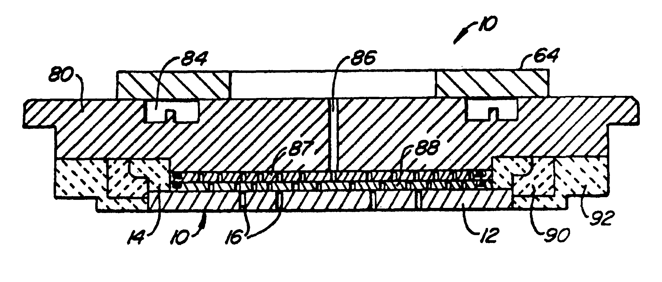
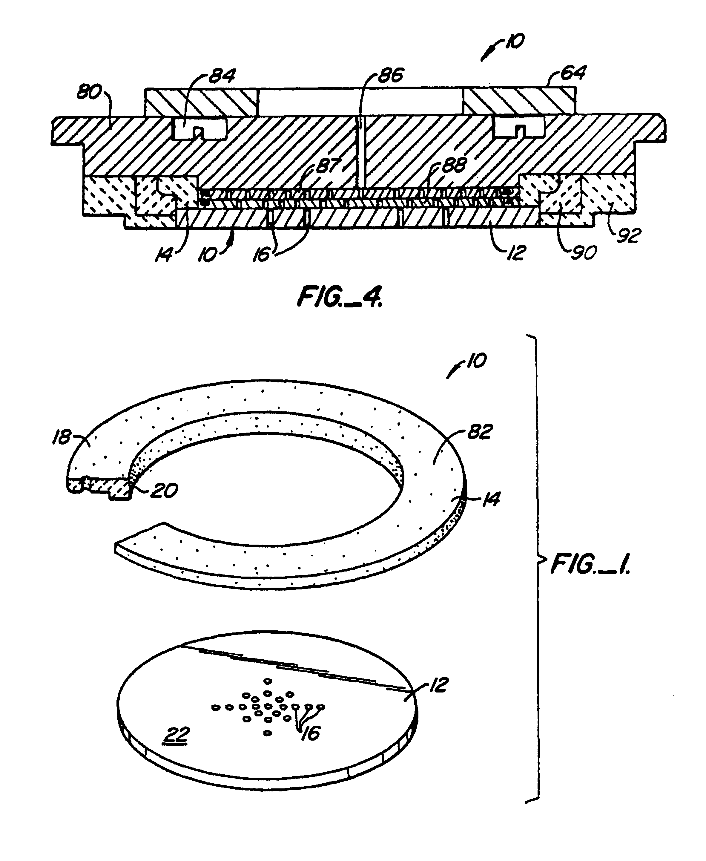
[0018]The present invention provides an improved construction for an electrode assembly useful particularly in parallel plate plasma reactor apparatus. Such reactor apparatus typically include upper and lower electrodes where the upper electrode is mounted in a housing which is capable of moving up and down relative to the lower electrode. The lower electrode which is generally fixed, will serve as a support service or “chuck” for the semiconductor wafer or other article which is being treated. A particular construction for such a reactor is described in more detail hereinafter with reference to FIG. 3.

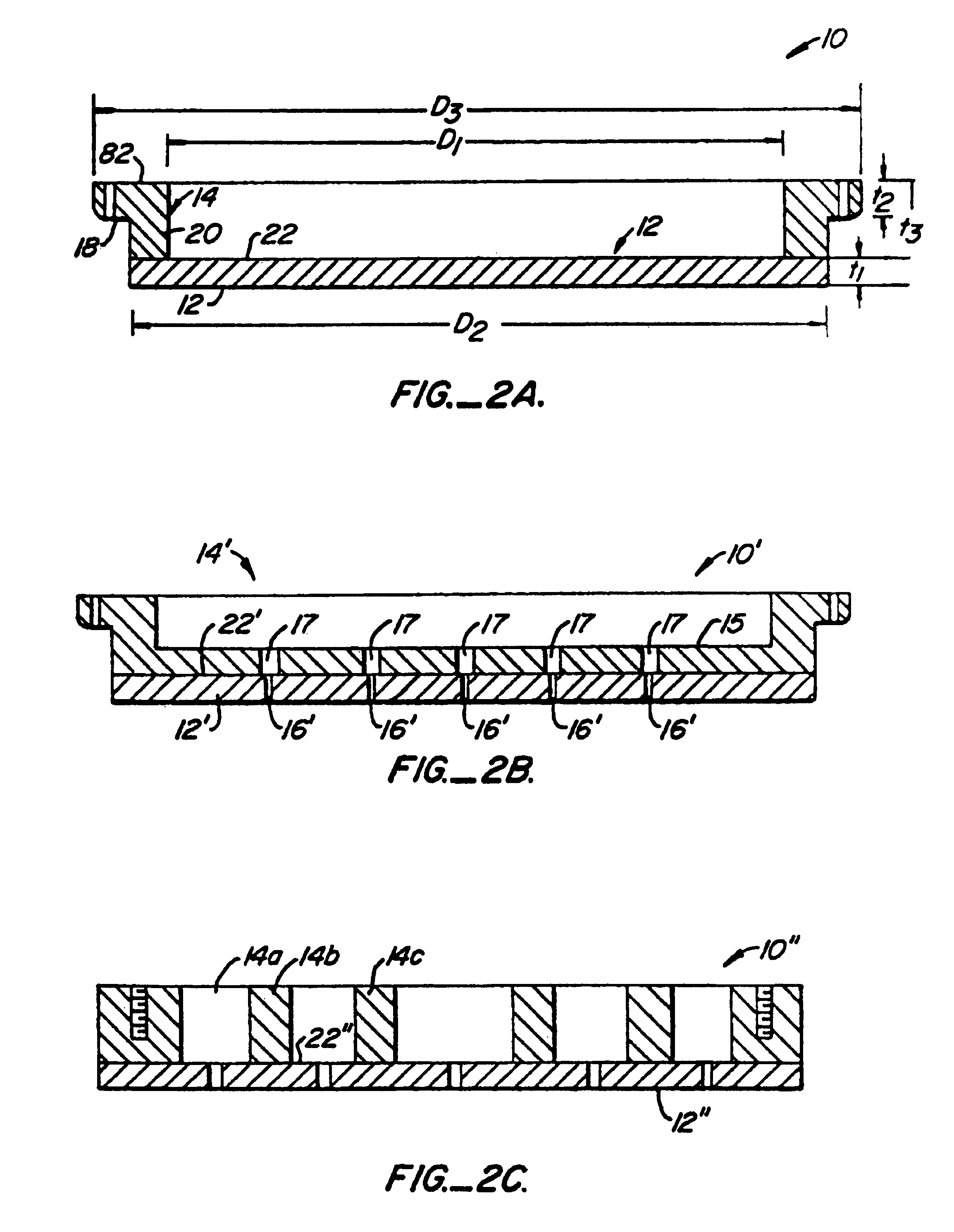
[0019]The electrode assembly of the present invention comprises a generally flat plate, usually in the form of a disk having a substantially uniform thickness thereacross, which is composed of a material which is “semiconductor pure”. Semiconductor purity means that the material is at least 99.999% pure and is substantially free of trace contaminants that could interfere with the asso...


PUM

PropertyMeasurementUnit
thicknessaaaaaaaaaa
thicknessaaaaaaaaaa
thicknessaaaaaaaaaa

Abstract

An electrode assembly for a plasma reactor, such as a plasma etch or plasma-enhanced chemical vapor deposition reactor, comprises an electrode plate having a support frame attached to one surface thereof. The electrode plate is composed of a substantially pure material which is compatible with a particular reaction being performed in the reactor, while the support frame is composed of a material having desirable thermal, electrical, and structural characteristics. The support frame is bonded to the electrode plate using a bonding layer, usually a ductile metallic bonding layer, which provides effective thermal and electrical coupling while permitting a degree of thermal expansion mismatch between the support frame and the electrode plate.

Description

[0001]1. Field of the Invention[0002]The present invention relates generally to the design of electrodes used for producing a plasma in a reactor vessel. More particularly, the present invention relates to the design of a composite electrode useful in plasma reactors, such as plasmid etch and plasma-enhanced chemical vapor deposition reactors.[0003]2. Description of the Background Art[0004]Plasma etching of semiconductor wafers and other substrates relies on the production of ionized gaseous species using a radio frequency (rf) discharge at pressures in the range from about 0.1 to 10 Torr, commonly referred to as a glow discharge. The charged species react with molecules at the surface of the substrate, resulting in volatile reaction products which are carried away.[0005]Several types of etchers are commonly employed in semiconductor fabrication including wet chemical (barrel) reactors, vertical dry chemical plasma reactors, and horizontal dry chemical plasma reactors. Of interest h...

Claims


Application Information

Patent Timeline
Patent Type & Authority Patents(United States)
IPC IPC(8): H01J37/32
CPCH01J37/32009H01J37/32532H01J37/3255Y10T29/49002Y10S156/914
Inventor DEGNER, RAYMOND L.LENZ, ERIC H.
Owner LAM RES CORP
Why Eureka
Try Eureka