Check patentability & draft patents in minutes with Patsnap Eureka AI!

Thin-film transistor array substrate structure

A technology of array substrate structure and thin film transistor, which is applied to transistors, electric solid state devices, semiconductor devices, etc., can solve the problems of general products without structure, and achieve the effect of improving performance

Inactive Publication Date: 2008-01-23
TPO DISPLAY
View PDF4 Cites 0 Cited by
  • Summary
  • Abstract
  • Description
  • Claims
  • Application Information

AI Technical Summary

Problems solved by technology

[0007] In order to solve the problems existing in the substrate structure of thin-film transistor arrays, relevant manufacturers have tried their best to find a solution, but no suitable design has been developed for a long time, and there is no suitable structure for general products to solve the above problems. This is obviously a problem that relevant industry players are eager to solve

Method used


Image

  • Thin-film transistor array substrate structure
  • Thin-film transistor array substrate structure
  • Thin-film transistor array substrate structure

Examples


Embodiment Construction

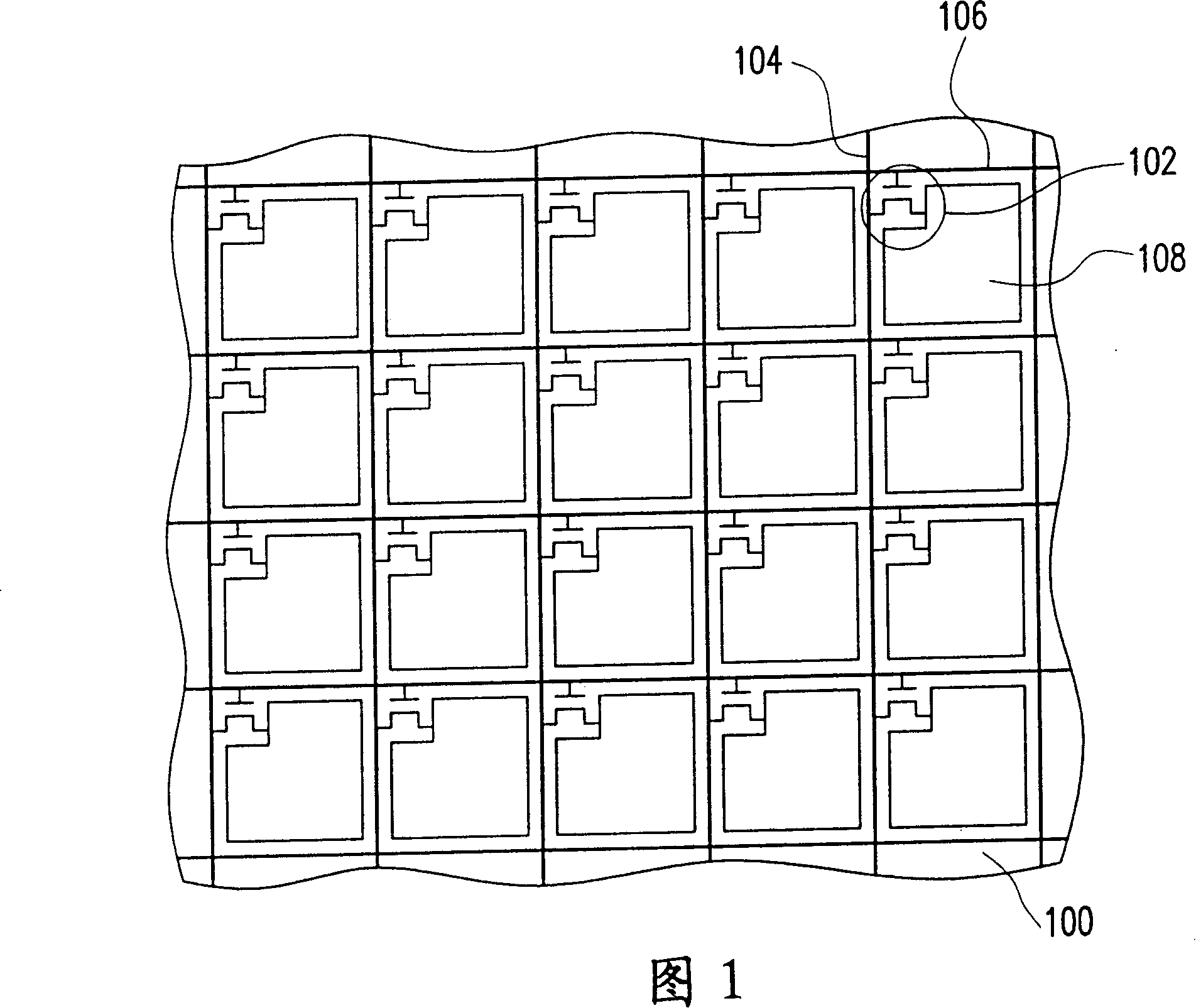
[0047] The specific implementation, structure, features and functions of the thin film transistor array substrate structure according to the present invention will be described in detail below with reference to the accompanying drawings and preferred embodiments.

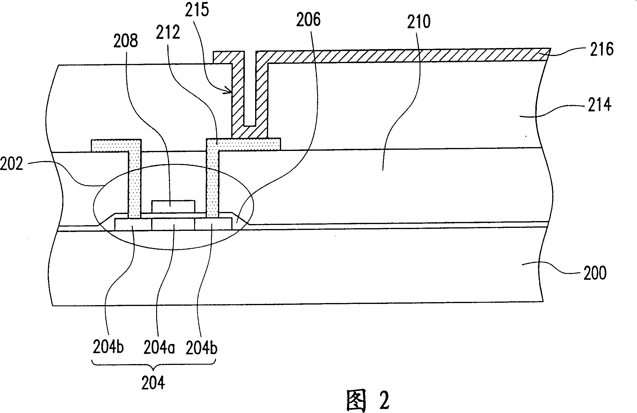
[0048] It is generally known that a dielectric layer of inorganic material, such as SiOx, SiNx, etc., is covered on the thin film transistor. Although the above-mentioned inorganic materials have a protective effect on the thin film transistor itself, they are not helpful to the film quality of the gate insulating layer in the thin film transistor. Therefore, in this embodiment, the hydrogen-containing dielectric layer is used as the inner dielectric layer, planar layer, reflective bump layer, or wide viewing angle bump layer on the thin film transistor, and the hydrogen-containing dielectric layer is used to repair the gate insulation. layer purpose.

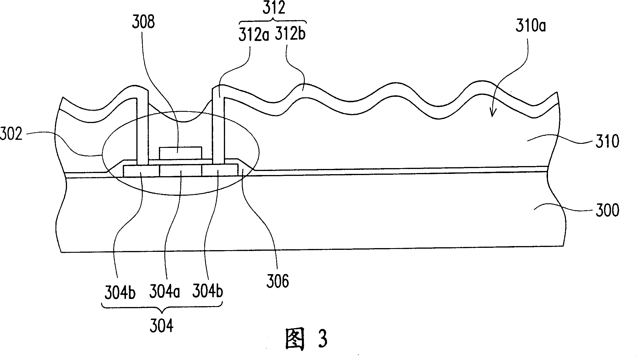
[0049] In this embodiment, only the top electrode type polysil...


PUM


Abstract

Structure of substrate of thin film transistor (TFT) array is composed of a transparent substrate, multiple TFTs, multiple scanning wires, multiple data wires, one or multiple layers of dielectric layer containing hydrogen and a patterned conductive layer. TFTs are configured on the transparent substrate. The layers of dielectric layer containing hydrogen configured on the transparent substrate cover the said TFTs, and patterned conductive layer is configured on dielectric layer containing hydrogen. Each TFT includes three terminals of poles of grid, source / drain. The grid pole is connected to the scanning wires, and source / drain poles are connected to the patterned conductive layer electrically. One or multiple layers of dielectric layer containing hydrogen are configured between grid metal layer and metal layer on the grid metal layer. Grid insulation layer is restored by hydrogen atom in dielectric layer containing hydrogen. Thus, efficiency of module is enhanced.

Description

technical field [0001] The present invention relates to a liquid crystal display structure in the field of electric digital data processing devices, in particular to a kind of arranging one or more hydrogen-containing dielectric layers between the gate metal layer and the metal layer above it, by hydrogen-containing The hydrogen atoms in the dielectric layer repair the gate insulating layer, thereby improving the performance of the device, and thus more suitable for a practical thin film transistor array substrate structure (TFT array, ie thin film transistor array substrate structure). Background technique [0002] The rapid progress of the multimedia society is mostly due to the rapid progress of semiconductor components or man-machine display devices. As far as the display is concerned, the cathode ray tube (Cathode Ray Tube, CRT) has been monopolizing the display market in recent years because of its excellent display quality and economical efficiency. However, for the ...

Claims


Application Information

Patent Timeline
IPC IPC(8): H01L29/786H01L27/12G02F1/136
Inventor 陈志宏陆一民
Owner TPO DISPLAY
Features
  • R&D
  • Intellectual Property
  • Life Sciences
  • Materials
  • Tech Scout
  • Unparalleled Data Quality
  • Higher Quality Content
  • 60% Fewer Hallucinations
Learn More