
Manufacturing method of a semiconductor integrated circuit device

A manufacturing method and semiconductor technology, applied in semiconductor/solid-state device manufacturing, semiconductor devices, electric solid-state devices, etc., can solve problems such as charge escape

Inactive Publication Date: 2008-02-13
RENESAS ELECTRONICS CORP
View PDF5 Cites 0 Cited by
  • Summary
  • Abstract
  • Description
  • Claims
  • Application Information

AI Technical Summary

Problems solved by technology

However, in the EEPROM with such a structure, if there is a defect in a certain part of the oxide film surrounding the floating gate electrode, since the charge storage layer is a conductor, all the charges stored in the storage node may escape due to abnormal leakage.

Method used


Image

  • Manufacturing method of a semiconductor integrated circuit device
  • Manufacturing method of a semiconductor integrated circuit device
  • Manufacturing method of a semiconductor integrated circuit device

Examples


Embodiment approach 1

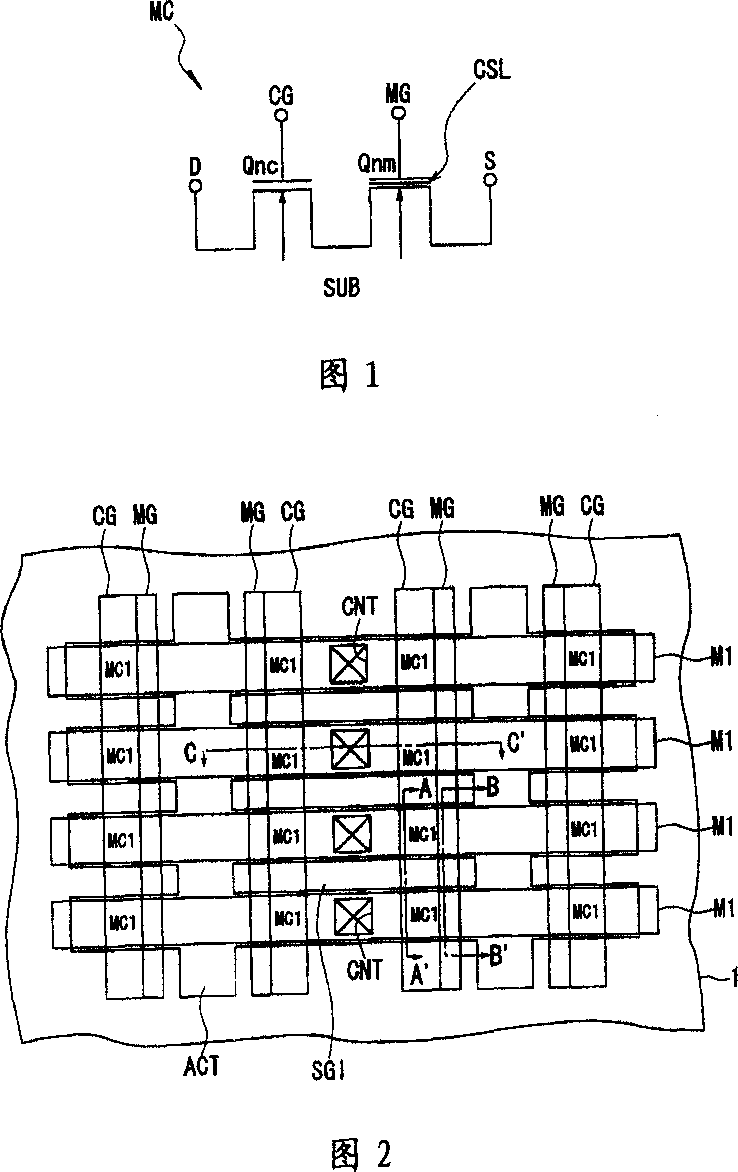
[0060] FIG. 1 shows a circuit diagram of a MONOS type memory cell.

[0061] The memory cell MC has, between the drain electrode D and the source electrode S, an nMISFET (first field effect transistor, hereinafter simply referred to as nMIS for selection) Qnc for memory cell selection, and an nMISFET (second field effect transistor for selection) Qnc for memory cells, for example. Field-effect transistors, hereinafter referred to only as nMIS for memory) Qnm 2 transistors. The nMISQnc for selection has a control gate electrode CG, and the nMISQnm for memory has a memory gate electrode MG and a charge storage layer CSL.

[0062] When performing a data readout operation, for example, about 1.0V is applied to the drain electrode D of the selected memory cell, about 1.5V is applied to the control gate electrode CG, and about 1.5V is applied to the source electrode S of the selected memory cell MC. For example, 0 (zero) V is applied to the memory gate electrode MG and the substrate...

Embodiment approach 2

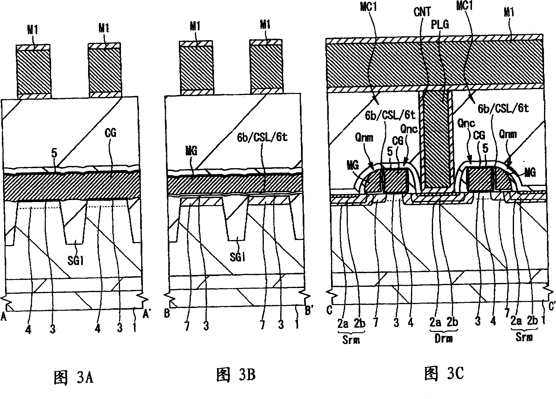
[0094] In Embodiment 2, an example in which the present invention is applied to a memory cell of the memory gate electrode-on-type will be described. FIG. 16 shows an example of a basic device cross-section of a memory cell in which a channel is cut along a direction intersecting the memory gate electrode MG (direction C-C' in FIG. 2 ). In Embodiment 1, two memory cells in the C-C' direction are shown, but in this embodiment, only one memory cell is shown for simplification of description.

[0095] The memory cell MC2 with the memory gate electrode on top has a planar structure substantially the same as that of the memory cell MC1 in Embodiment 1, but has a cross-sectional structure in which a part of the memory gate electrode MG is placed between the control gate electrode CG. On one side, insulation of the control gate electrode CG and the memory gate electrode MG is formed by the insulating film 18 made of silicon oxide or the like, the insulating films 6b, 6t, and the char...

Embodiment approach 3

[0103] In Embodiment 3, an example in which the present invention is applied to a control gate electrode-on-type memory cell will be described. FIG. 21 shows a cross-sectional view of the main part of the memory cell, and FIG. 22 shows the basic device of the memory cell in which the channel is cut along the direction (DD' line of FIG. 21 ) crossing the memory gate electrode. An example of a section.

[0104] In active region ACT on the main plane of substrate 1, nMISQnc for selection and nMISQnm for memory of memory cell MC3 are arranged. On the main plane of the substrate 1 between the drain region Drm and the source region Srm of the memory cell MC3, the control gate electrode CG of the selection nMISQnc and the memory gate electrode MG of the memory nMISQnm extend adjacently, and the control A part of the gate electrode CG is located on the side of the memory gate electrode MG. In addition, similarly to the memory cell MC1 in Embodiment 1 described above, in the extendin...


PUM


Abstract

Provided is a technique for improving reliability, specially, a data holding characteristic for a semiconductor device having a nonvolatile memory using a nitride film as a charge accumulation layer.On a 1st area of a substrate (1), a control gate electrode (CG) of nMISQnc for selection is formed across a gate insulating film (3) and on a 2nd area, a charge storage layer (CSL) of nMISQnm for memory is formed across an insulating film (6b) so that its content hydrogen density is 1020cm-3. After an insulating film (6t) is further formed, a memory gate electrode (MG) of nMISQnm for memory is formed across the insulating films (6b and 6t) and charge storage layer (CSL) and impurities are injected into an area where the nMISQnc for selection and nMISQnm for memory are adjacent to form a semiconductor area (2a) constituting the drain area Drm and source area Srm of a memory cell.

Description

technical field [0001] The present invention relates to a semiconductor device and its manufacturing technology, in particular to a technology effective for a semiconductor device having a MONOS (Metal Oxide Nitride Oxide Semiconductor) structure with a nitride film as a charge storage layer. Background technique [0002] EEPROM (Electrically Erasable Programmable Read Only Memory, Electrically Erasable Programmable Read Only Memory) or flash memory and other electrically rewritable non-volatile memory, because the program can be rewritten on the circuit board, so in addition to shortening the In addition to improving the development cycle and development efficiency, it has also been extended to various applications such as low-volume high-variety production, adjustment by shipping location, and program update after shipment. Especially in recent years, there has been a great demand for a microcomputer incorporating an MPU (Micro Processing Unit) and an EEPROM (or flash memo...

Claims


Application Information

Patent Timeline
Patent Type & Authority Patents(China)
IPC IPC(8): H01L21/8247H01L21/336H01L27/115H01L29/792H01L29/788H10B20/00H10B69/00
CPCH01L29/792H01L27/115H01L27/11568H10B69/00H10B43/30
Inventor 佐藤英纪冈崎勉
Owner RENESAS ELECTRONICS CORP
Learn More