Thin film transistor display array measuring circuit and method
A thin film transistor and testing circuit technology, applied in the field of pixel storage capacitor testing, can solve the problems of time-consuming, insufficient reliability, weak signal, etc.
- Summary
- Abstract
- Description
- Claims
- Application Information
AI Technical Summary
Problems solved by technology
Method used
Image

Examples
Embodiment Construction
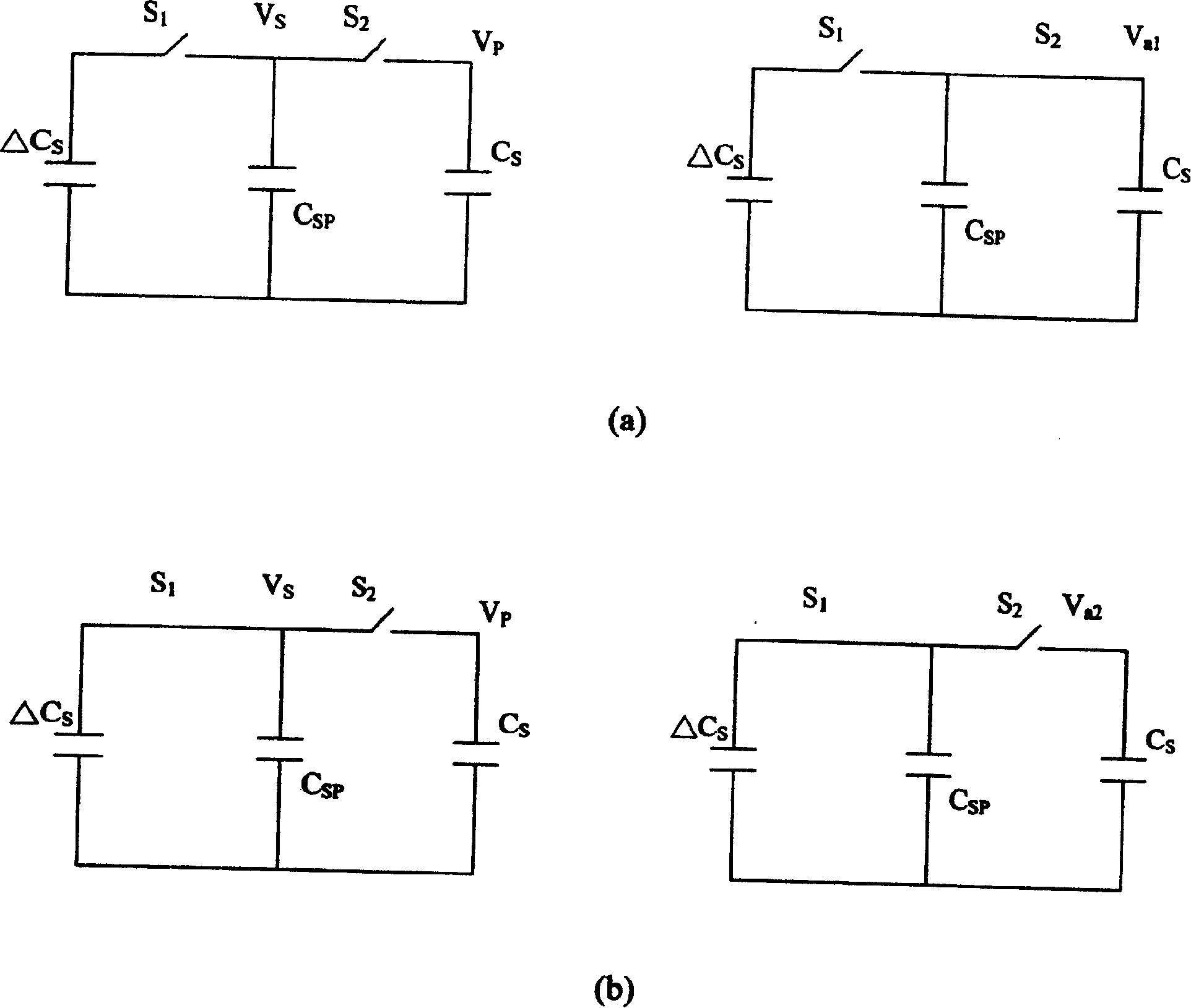
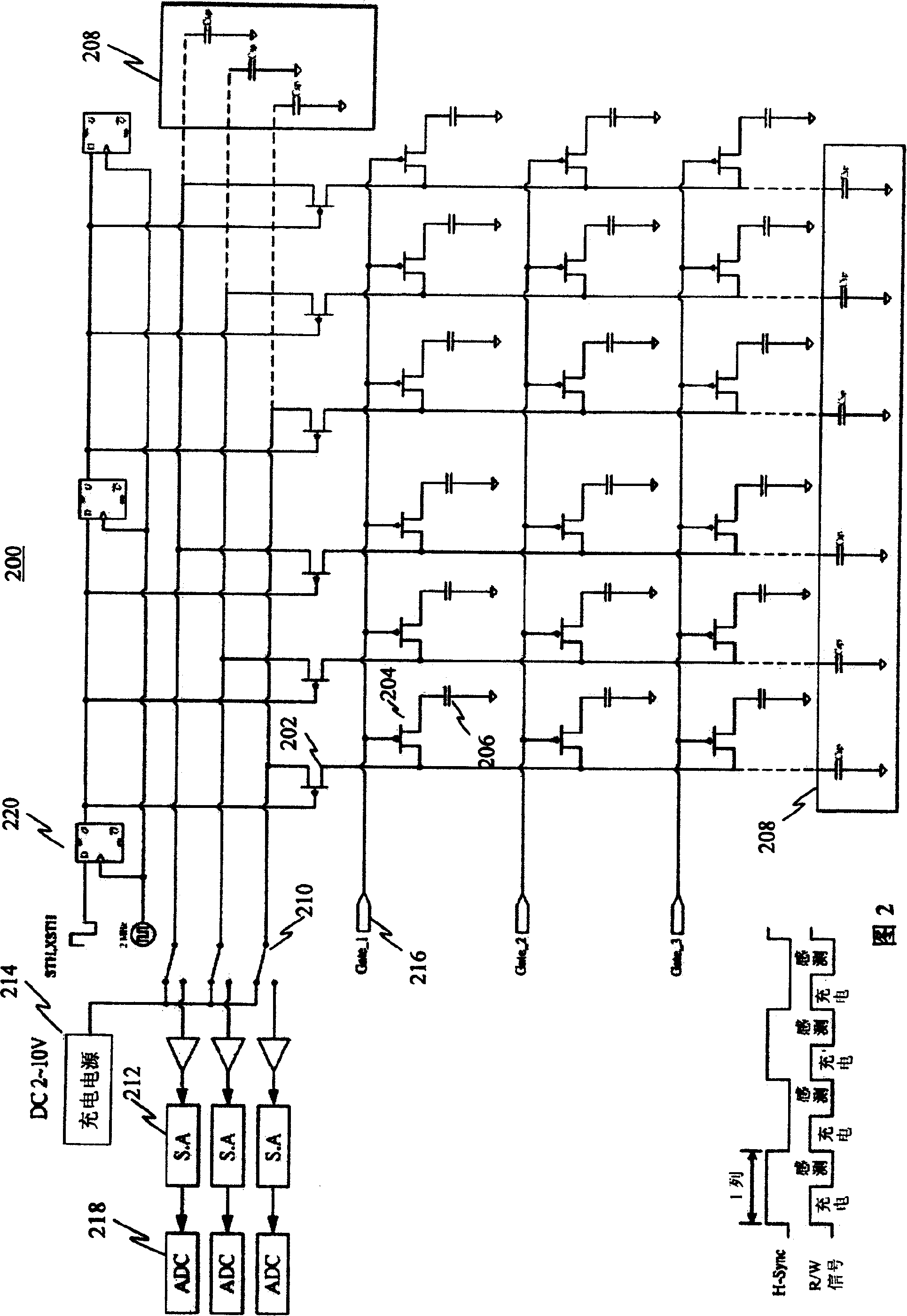
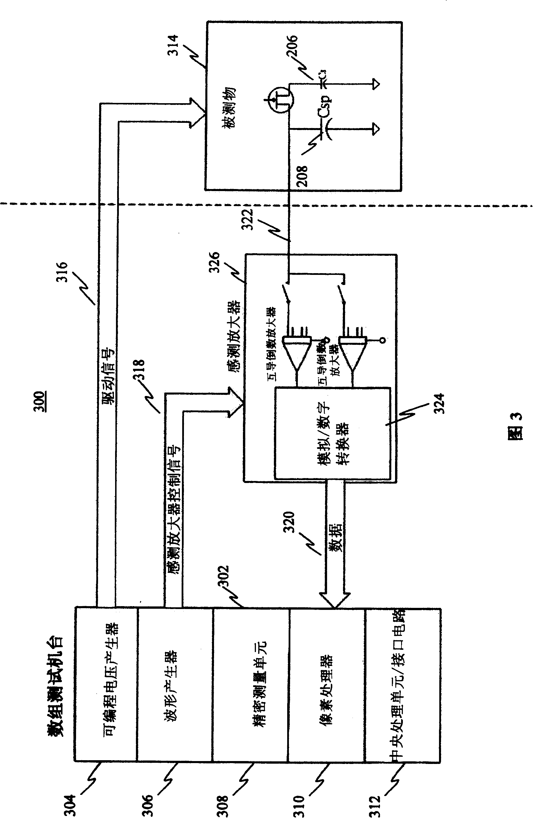
[0041] The content of the present invention can be disclosed through the description of the following embodiments and related drawings. FIG. 2 is a schematic connection diagram of a test circuit 200 for a display circuit of a low temperature polysilicon (Low Temperature Poly-Si) thin film transistor array according to an embodiment of the present invention. Row switch transistor 202 or claim read / write switch transistor, accept the control closed circuit (ON) or open circuit (OFF) of its gate of row switch gate control circuit 220, so that DC charging power supply 214 or test circuit is connected by source and drain Connected to the row, for example, the nth row (n=1 to N, N being the total number of rows), the gate of the pixel switch transistor 204 is connected to the column control column of the kth column (k=1 to K, K being the total number of columns). Gate circuit 216, the source of the pixel switching transistor 204 is connected to the drain of the row switching transis...
PUM
 Abstract
Description
Claims
Application Information
 - R&D
- Intellectual Property
- Life Sciences
- Materials
- Tech Scout
- Unparalleled Data Quality
- Higher Quality Content
- 60% Fewer Hallucinations
Browse by: Latest US Patents, China's latest patents, Technical Efficacy Thesaurus, Application Domain, Technology Topic, Popular Technical Reports.
© 2025 PatSnap. All rights reserved.Legal|Privacy policy|Modern Slavery Act Transparency Statement|Sitemap|About US| Contact US: help@patsnap.com