
Three-dimensional microstructure electroforming method and apparatus

A microstructure and electroforming technology, applied in electrophoretic electroforming and other directions, can solve the problems of difficulty in degumming, long processing cycle, rough surface, etc., and achieve easy automation and mass production, high replication accuracy and repeatability, and rough surface. small effect

Inactive Publication Date: 2008-06-18
NANJING UNIV OF AERONAUTICS & ASTRONAUTICS
View PDF4 Cites 0 Cited by
  • Summary
  • Abstract
  • Description
  • Claims
  • Application Information

AI Technical Summary

Problems solved by technology

However, the technology has many steps, the process is complicated, and the microstructure materials produced are limited, currently only limited to metal nickel
LIGA technology needs to use extremely expensive and scarce synchrotron radiation light source, which has high cost and long processing cycle; micro-electroforming is prone to defects such as uneven thickness, loose structure, pinholes, and rough surface; quasi-LIGA technology cannot obtain high aspect ratio. Microstructure, and the photoresist stress is large, and it is difficult to remove the glue; due to the use of the tip effect of the electric field in local electrochemical deposition, the microstructure of the metal microstructure obtained is loose, and only a small number of special-shaped parts can be produced; the electrodes of micro-EDM Loss and compensation issues have not been well resolved

Method used


Image

  • Three-dimensional microstructure electroforming method and apparatus
  • Three-dimensional microstructure electroforming method and apparatus

Examples


Embodiment Construction

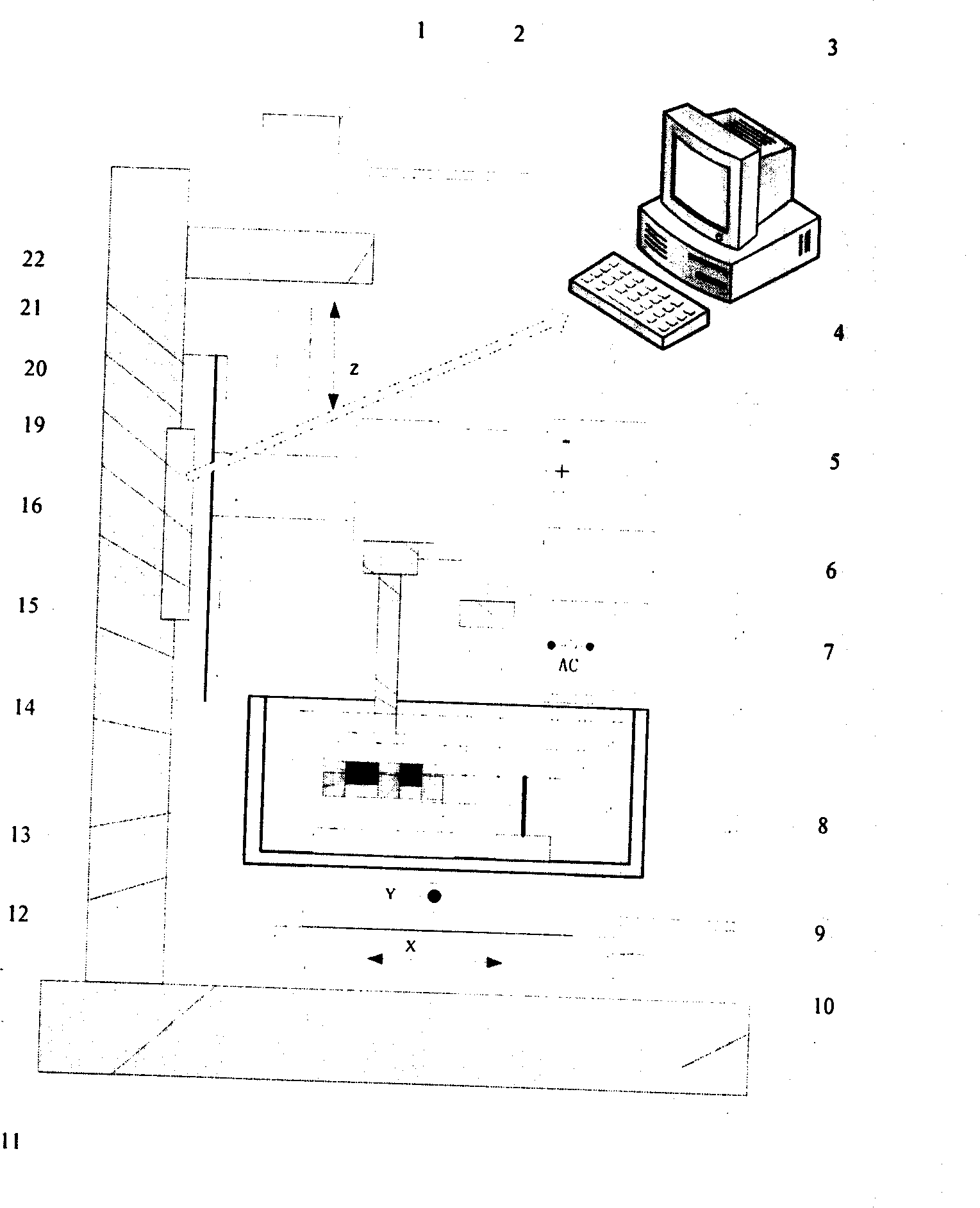
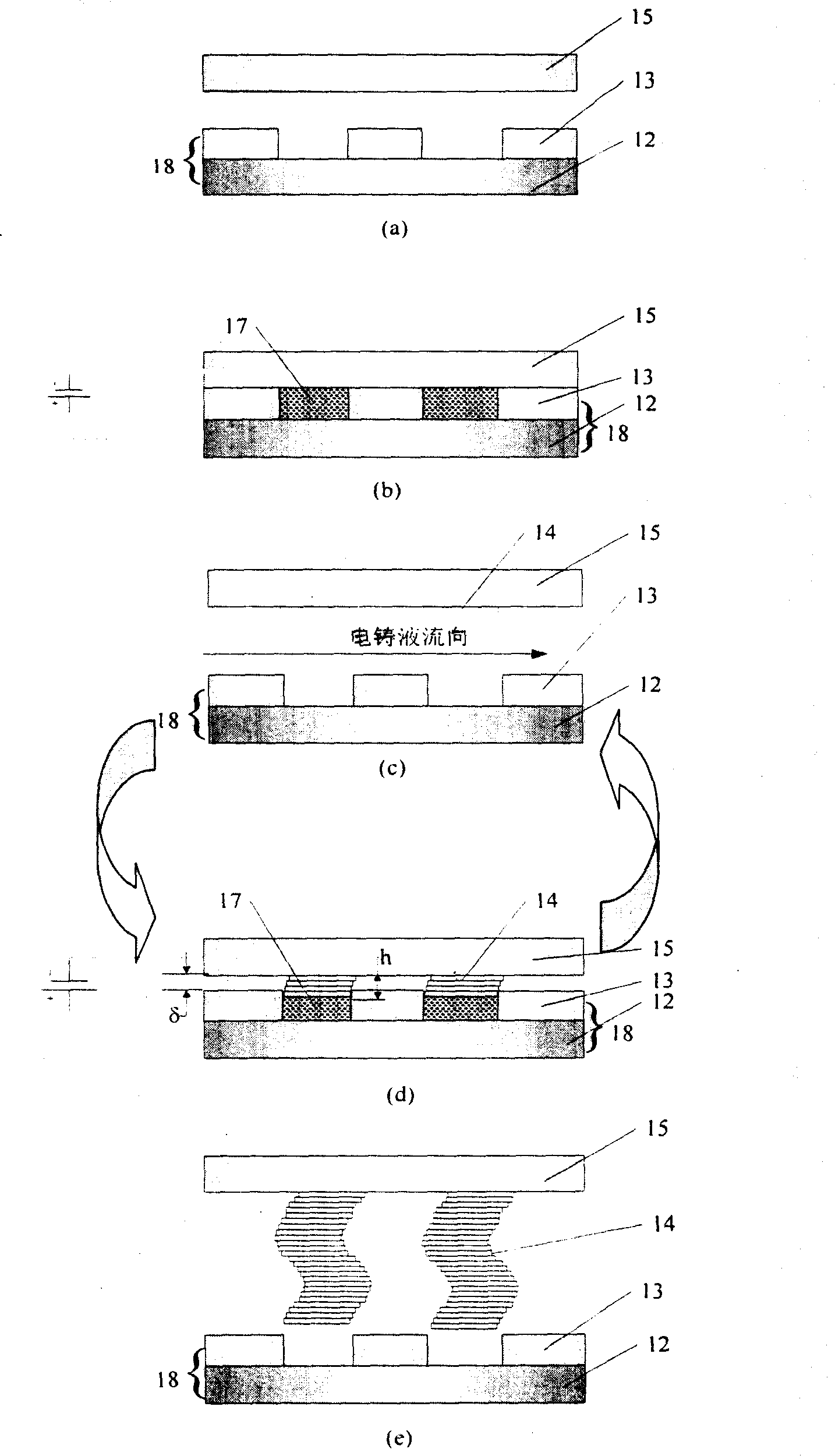
[0029] according to figure 1 As shown, the "three-dimensional microstructure electroforming device" of the present invention includes a motor 1 , a power supply 4 , a temperature controller 5 , a heater 6 , a temperature sensor 7 , an electroforming tank 8 , and a machine tool body 10 . Its characteristics are: the computer 3 controls the on-off of the electronic switch 22 to realize the power supply 4 for the electroforming branch and the online measurement branch respectively; the shielding anode film plate 18 is composed of the anode substrate 12 and the shielding film 13, and passes through the anode The installation fixture 11 is installed on the CNC workbench 9, and the cathode 15 is properly connected to the Z-axis 2; during electroforming, the computer 3 controls the Z-axis 2 and the CNC workbench 9 to move accordingly, so as to drive the shielding anode film plate 18 Make relative movement with the cathode 15; during online measurement, the computer 3 controls the Z-a...


PUM


Abstract

The invention relates the three-dimensional fine structure electrocasting and device, belonging to micro handling field. The method uses barrier anode film plate to limit electrodeposition. Computer controls electrical source to make the electrodeposition progress at intervals. At non-electrical deposition, the barrier anode film plate and cathode relative move, define the relative dislocation according to element configuration shape. At every beginning of deposition cycle, define the relative dislocation at Z direction to guarantee that sedimentary deposit surface is lower than glue line surface. The apparatus key is the connection of electroforming device and digital controller, the relative dislocation of barrier anode film plate and cathode anode film and the on-line measurement of the deposit height. The invention has the advantages of fine and close structure, straight side panel and low cost.

Description

technical field [0001] The three-dimensional microstructure electroforming method and device of the invention belong to the field of micromachining. Background technique [0002] Micro Electro Mechanical System (MEMS) is one of the most important scientific and technological advances in the 20th century, and it is also a hot spot of scientific research today. Micro-manufacturing technology is the foundation and core of MEMS. High-Aspect-Ratio Microstructures (HARMS) with high aspect ratio (or called aspect ratio) are widely used in MEMS. The manufacturing level of HARMS often directly affects or even determines the performance and characteristics of micro-devices. A high aspect ratio may bring higher sensitivity, greater displacement or stronger driving force to micro-devices. For example: In order to obtain as large an output torque or energy as possible in a certain micro size in magnetic drives, micro motors and miniature eddy current sensors, it is necessary to increas...

Claims


Application Information

Patent Timeline
Patent Type & Authority Patents(China)
IPC IPC(8): C25D1/12
Inventor 朱荻曾永彬曲宁松
Owner NANJING UNIV OF AERONAUTICS & ASTRONAUTICS
Learn More